Absorption spectra of T = 0K semiconductor?

In summary, the absorption spectrum of a T=0K intrinsic semiconductor is determined by the density of states for the valence and conduction bands, which are given by E_v(k) = -\hbar^2 k^2/2m_v and E_c(k) = E_g + \hbar^2 k^2/2m_c, respectively. The absorption spectrum is not directly related to the product of these densities, but instead is determined by the energy difference between the conduction and valence bands at a given value of the vector k. This is represented by the joint density of states, which enforces that the transitions take place vertically in k space. Ultimately, the absorption spectrum varies linearly with the energy
  • #1
AntiElephant
25
0
I'm trying to understand the form of the absorption spectrum of a T=0K intrinsic semiconductor. The valence band/conduction band energy diagram looks like;

http://postimg.org/image/wyzvo9lsr/
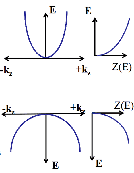
Untitled.png


As [itex] E = \frac{\hbar^2 k^2}{2m^*} [/itex]

where [itex] m^* [/itex] denotes the effective mass. The image doesn't indicate too well that the effective mass in the valence band is MUCH larger than that in the conduction band.

I'm trying to understand the absorption spectrum of photons sent into the semiconductor. For photons with energy less than the band gap there is no absorption.

When photons with energy more than the band gap are sent in, there is absorption. We assume that the momentum of the photons is low and so in the diagram above there can only be vertical transitions from the valence to the conduction band - so the transition energies are uniquely determined (i.e. an electron is promoted from [itex] E_2 [/itex] to [itex] E_1 [/itex] and [itex] E_1,E_2[/itex] are uniquely determined).

I would hazard a guess that the absorption spectrum is proportional to the product of the density of states [itex] Z(E_1)Z(E_2) [/itex]. There are two ways I can interpret this...

1) Examine the change of the absorption spectrum from a photon energy [itex] E [/itex] to a small increase [itex] E + \Delta E [/itex]. For a vertical transition, [itex] E_2 [/itex] barely changes because the effective mass in the valence band is so large, but [itex] E_1 [/itex] changes quite rapidly since it is so low in the conduction band. So [itex] Z(E_2) [/itex] is practically constant and so the absorption spectra depends only on [itex] Z(E_1) [/itex]. Since [itex] Z(E_1) \propto E_1^{1/2} [/itex] we see the absortion spectrum increase like [itex] E^{1/2} [/itex].

2) Mathematically you can see, since the momentum is conserved

[itex] E_1 = \frac{\hbar^2 k^2}{2m_c^*} [/itex]
[itex] E_2 = \frac{\hbar^2 k^2}{2m_v^*} [/itex]

[itex] E_1/E_2 = m_v^*/m_c^* [/itex]

Then the absorption rate is [itex] \propto Z(E_1)Z(E_2) \propto (E_1 E_2)^{1/2} \propto E_1 [/itex]

And so it varies linearly with [itex] E_1 [/itex] and hence the energy of the photon.


I'm told actually it varies like [itex] E^{1/2} [/itex] which would imply the second way is wrong. But how does the maths lie?

{Edit: I've included the image so that one doesn't have to click the link to see it - Zz}
 
Last edited by a moderator:
Physics news on Phys.org
  • #2
We have to be a bit more careful in definitions here. From your figure, you can see that valence band dispersion is given by [itex]E_v(k) = -\hbar^2 k^2/2m_v[/itex] and the conduction band is given by [itex]E_c(k) = E_g + \hbar^2 k^2/2m_c[/itex]. From this you can work out the density of states for each band (there is indeed a square root involved) - but importantly, the density of states for the valence band vanishes where the density of states for the conduction band is nonzero, and vice versa. This should convince you that absorption is not related to the product of the densities of states. Instead, think about the energy difference [itex]E_c(k)-E_v(k)[/itex] for each [itex]k[/itex] ... this should lead you to a quantity called the "joint density of states" which is indeed closely related to absorption.
 
  • #3
t!m said:
We have to be a bit more careful in definitions here. From your figure, you can see that valence band dispersion is given by [itex]E_v(k) = -\hbar^2 k^2/2m_v[/itex] and the conduction band is given by [itex]E_c(k) = E_g + \hbar^2 k^2/2m_c[/itex]. From this you can work out the density of states for each band (there is indeed a square root involved) - but importantly, the density of states for the valence band vanishes where the density of states for the conduction band is nonzero, and vice versa. This should convince you that absorption is not related to the product of the densities of states. Instead, think about the energy difference [itex]E_c(k)-E_v(k)[/itex] for each [itex]k[/itex] ... this should lead you to a quantity called the "joint density of states" which is indeed closely related to absorption.

I apologise but I'm still lost. Even with the clean up of definitions I run into the same issue.

Using [itex]E_v(k) = -\hbar^2 k^2/2m_v[/itex], [itex]E_c(k) = E_g + \hbar^2 k^2/2m_c[/itex] as you said. One then gets [itex] E_c(k) - E_v(k) = E_{\gamma} [/itex] which, for a given [itex] E_{\gamma}, E_g [/itex], fixes the constant k. This, in turn, fixes [itex] E_c(k) [/itex] and [itex] E_v(k) [/itex].

I get that the valence band DoS vanishes where the conduction band DoS is zero. But I don't get how this means the absorption magnitude is not related to the product of the two. I'm not using [itex] Z_v(E)Z_c(E) [/itex] where [itex] E [/itex] is a fixed energy. I'm using [itex] Z_v(E_2)Z_c(E_1) [/itex] where [itex] E_1 = E_c(k) [/itex], [itex] E_2 = E_v(k) [/itex].

I imagine the absorption magnitude is a product of the number of electrons states that can take that photon energy (proportional to [itex] Z_v(E_2) [/itex]) and the number of electrons states they can be promoted to (proportional to [itex] Z_c(E_1) [/itex]). So the absorption magnitude would proportional to the product of [itex]Z_c(E_1)Z_v(E_2)[/itex]...?

Ideally [itex] Z_c(E_c(k)) \propto (E_c(k) - E_g)^{1/2} \propto k [/itex]. [itex] Z_v(E_v(k)) \propto (-E_v(k))^{1/2} \propto k [/itex]

Then [itex] Absorption~magnitude \propto k^2 \propto E_{\gamma} - E_G[/itex]. Where [itex] k^2 \propto E_{\gamma} - E_G[/itex] is seen by re-arranging [itex] E_c(k) - E_v(k) = E_{\gamma} [/itex]. So it varies linearly with [itex] E_{\gamma} [/itex]?
 
Last edited:
  • #4
The problem with taking the product of the individual densities of states is that you are not enforcing that the transitions take place at a given value of the vector [itex]k[/itex]. Remember that the density of states is only a function of energy, not [itex]k[/itex]; it is only for the free electron (parabolic) dispersion can you invert to get the magnitude of [itex]k[/itex] given the energy (but you can not invert to get the vector [itex]k[/itex]). So in some sense you are overcounting by taking the product as you suggest, because you are counting transitions which are not vertical in the vector space of [itex]k[/itex]. What you want is the joint density of states which enforces that the transitions happen vertically in [itex]k[/itex] space,
[tex] JDOS(E) = \int d^3k\ \delta(E_c(k)-E_v(k)-E) [/tex]
 
  • Like
Likes 1 person

FAQ: Absorption spectra of T = 0K semiconductor?

What is the significance of studying the absorption spectra of T = 0K semiconductors?

Studying the absorption spectra of T = 0K semiconductors allows scientists to understand the electronic structure and energy levels of the material. This information is crucial in developing and optimizing electronic devices such as transistors and solar cells.

How is the absorption spectra of T = 0K semiconductors measured?

The absorption spectra of T = 0K semiconductors is typically measured using spectroscopy techniques, such as UV-Vis or infrared spectroscopy. These techniques involve shining light of different wavelengths onto the material and measuring the intensity of light that is absorbed.

What does the absorption spectra of T = 0K semiconductors tell us about the material?

The absorption spectra of T = 0K semiconductors provides information about the band gap energy, which is the energy required for an electron to move from the valence band to the conduction band. It also reveals the material's absorption coefficient, which is a measure of how strongly the material absorbs light at a specific wavelength.

How does temperature affect the absorption spectra of semiconductors?

As the temperature increases, the absorption spectra of semiconductors shifts towards longer wavelengths due to thermal excitation of electrons. This is known as the redshift effect. At T = 0K, the absorption spectra provides information about the fundamental electronic structure of the material without any thermal effects.

How is the absorption spectra of T = 0K semiconductors used in practical applications?

The absorption spectra of T = 0K semiconductors is used to design and optimize electronic devices, such as transistors, solar cells, and LEDs. It also helps in identifying and characterizing new semiconductor materials that may have unique properties for specific applications.

Similar threads

Replies
11
Views
1K
Replies
4
Views
2K
Replies
3
Views
2K
Replies
9
Views
7K
Replies
12
Views
2K
Replies
1
Views
2K
Replies
7
Views
3K
Back
Top