Band Bending at SiO2 Interface

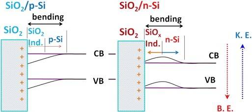
In summary, the conversation is discussing band bending in a semiconductor at the SiO2 interface. The picture shows how the binding energy (B.E.) and kinetic energy (K.E.) of charges change. The question is what happens to the total energy of charges in band bending. The conversation also mentions that the picture is a schematic representation of band-bending in SiO2/p-Si and SiO2/n-Si interfaces and that B.E. and K.E. refer to binding and kinetic energies. The question is how band-bending causes the change from B.E. to K.E. or vice versa for electrons/holes.
  • #1
1msm
8
0
Hello everyone !

In below picture we can see band bending in semiconductor at SiO2 interface,
as show in picture how charge's BE(binding energy) and KE(kinetic energy) are changing..??
Or what happens to charges total energy in band bending ..??

BE-KE.jpg


\\
 
Physics news on Phys.org
  • #2
1msm said:
Hello everyone !

In below picture we can see band bending in semiconductor at SiO2 interface,
as show in picture how charge's BE(binding energy) and KE(kinetic energy) are changing..??
Or what happens to charges total energy in band bending ..??

Please re-read what you wrote. These appear to be statements that just happen to end with "?". What EXACTLY are you asking for here?

Zz.
 
  • #3
Sorry for the inconvenience,

the above picture is a Schematic representation of band-bending in SiO2/p-Si and SiO2/n-Si interfaces.
B.E. and K.E. refer to binding and kinetic energies respectively.

this is the only small information available from it.

Now my question is,
How exactly the band-bending causes the electrons/holes energy to change from B.E to K.E or from K.E to B.E ?
 

FAQ: Band Bending at SiO2 Interface

1. What is band bending at the SiO2 interface?

Band bending at the SiO2 interface is a phenomenon that occurs at the interface between a silicon (Si) substrate and a layer of silicon dioxide (SiO2) on its surface. It refers to the change in the energy levels of the conduction and valence bands of the Si substrate due to the presence of the SiO2 layer.

2. Why does band bending occur at the SiO2 interface?

Band bending occurs at the SiO2 interface due to the difference in the dielectric constants of Si and SiO2. The SiO2 layer has a higher dielectric constant, which creates an electric field at the interface, causing a shift in the energy levels of the Si substrate.

3. How does band bending affect the electronic properties of the Si substrate?

Band bending can affect the electronic properties of the Si substrate in various ways. It can change the effective mass of electrons and holes, alter the band gap, and affect the carrier concentration and mobility, all of which ultimately impact the overall performance of electronic devices.

4. What factors influence the magnitude of band bending at the SiO2 interface?

The magnitude of band bending at the SiO2 interface can be influenced by several factors, such as the thickness and doping concentration of the Si substrate, the thickness and dielectric constant of the SiO2 layer, and the type of metal used in the gate electrode of a transistor.

5. How is band bending measured and characterized?

Band bending can be measured and characterized through various techniques, such as capacitance-voltage (C-V) measurements, Kelvin probe force microscopy (KPFM), and x-ray photoelectron spectroscopy (XPS). These techniques can provide information about the energy level shifts and band gap changes at the SiO2 interface.

Similar threads

Back
Top