Constructing a JK Flip-Flop: Troubleshooting Unexpected Outputs

In summary, the conversation discussed the construction of a JK flip-flop using basic NAND gates and the issues faced by different groups with the expected values of Q and Q' based on the input values. Some groups also faced issues with the toggle state always giving Q=Q'=1. The errors were occurring randomly and changing ICs often resulted in getting wrong outputs for different input values. One group tried to recreate the issue at home and used a 5V supply from an Arduino Mega. They consistently got the same values for Q and Q' for different input values. There was a discussion about using a master-slave JK flip-flop to solve the issue and the use of debounced logic drive for input levels. The conversation also mentioned the
  • #1
Wrichik Basu
Science Advisor
Insights Author
Gold Member
2,138
2,713
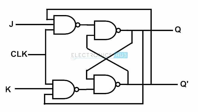
Our exercise in lab today was to construct a JK flip-flop using basic NAND gates. The ICs we used were 74LS00 and 74LS10. The circuit diagram we used is this:
jk.jpg

We were, however, not getting the expected values of Q and Q' based on the values of J, K and CLK. For instance, in my case, CLK=1, J=1 and K=0 gave Q=1, as expected. But the moment I put CLK to GND, both Q and Q' went up to the HIGH state, irrespective of the values of J and K. We checked our circuit as well as the ICs, but there was no fault in either one.

Some other groups were facing the same issue as us, although for some specific set of input values only. Other groups were facing a different issue: suppose after setting J=1 and K=0, when they set J=1 and K=1 (the toggle state), both outputs went up to 1. In short, the toggle state was always giving Q=Q'=1.

The errors were occurring randomly, in the sense that not all groups had the exact same wrong output for a particular set of input values. If a group changed ICs, they often got the wrong output(s) for a different set of input values.

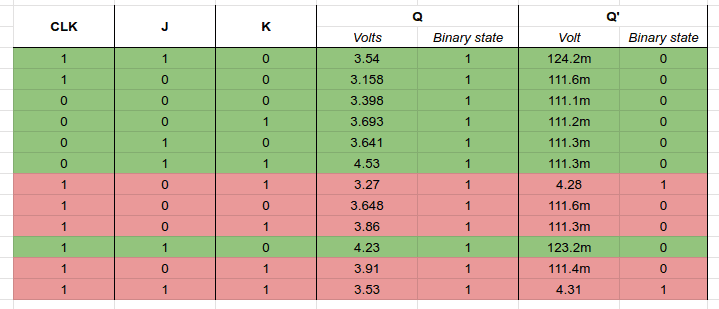
I brought two ICs home to see if I can re-create the issue. I used a 5V supply from an Arduino Mega. This is what I got:
1680292065738.png

The green rows indicate that the measured state is the same as the expected state. Red indicates that the measured state and expected state does not agree. The inputs are written exactly in the sequence they were applied. Hence, some input values are repeated. A number followed by "m" implies mV, otherwise V.

As you may see, this is not the same as what I got in class today. But I was getting the values consistently. E.g., if I set CLK=1, J=1 and K=1, I consistently got Q=Q'=1 irrespective of what the previous state was.

Some of my classmates were saying that a master-slave JK flip-flop will solve this. The Prof. hasn't given any answer yet.

Why is this happening? Race condition between the transistors used in the ICs? What can we do to prevent this?
 
Physics news on Phys.org
  • #2
What logic gates were used for this circuit (family, number)? You show both 2-input and 3-input devices. Were there 2 different ICs used? If so, were all unused inputs tied off to either high or low?

How are the input levels being driven into the gates? Are you just using switches, or debounced logic drive?
 
  • Like
Likes scottdave
  • #4
berkeman said:
What logic gates were used for this circuit (family, number)?
74LS00 and 74LS10.
berkeman said:
Were there 2 different ICs used?
Yes.
berkeman said:
If so, were all unused inputs tied off to either high or low?
No, unused inputs were kept floating.
berkeman said:
How are the input levels being driven into the gates? Are you just using switches, or debounced logic drive?
No switches. Just unplugging and plugging wires into 5V and GND rails.

Also, just for clarification, we didn't use any crystal for the clock input; it was manually switched between 0 and 1. In addition, in the circuit I made at home, I did put a 0.1μF ceramic capacitor between Vcc and GND for each IC.
 
  • #5
TTL is a current sinking, negative logic. You must learn to think backwards and upside down.
TTL lesson 1. A low input is when current flows out of the input to ground. A high is when current does not flow out of the input.
TTL lesson 2. It is current that is important, not voltage. Voltages less than 0.80 volt are probably low, greater than 1.2 volts are probably high. Make it easier to differentiate high and low by tying floating outputs to +5 volts through a 2k2 pull-up resistor.
TTL lesson 3. An unused high input should not be connected directly to the +5 volt supply rail without a series resistor ≥ 1k. That protects the input from a momentary overvoltage on the supply that can injure the input transistor. Most beginners ignore that, until they have wasted a few days trying to debug a TTL circuit with a damaged input.

A clock input should be "de-bounced" so there is only one edge. Use a two position toggle switch to ground only one input at the time of an RS flip-flop, made from two 74LS00 NAND gates, with pull-up resistors on the inputs.
 
  • Informative
  • Like
Likes scottdave, Wrichik Basu and berkeman
  • #6
Wrichik Basu said:
No, unused inputs were kept floating.
With old TTL logic gates, you can probably get away with this, but in general with CMOS circuitry, always tie off unused inputs. It's a good design practice, and will help you with interview questions. :wink:

Anyway, did you see the text in the HyperPhysics piece that I posted? That pretty much answers your questions.
 
  • Like
Likes scottdave and Wrichik Basu
  • #7
Baluncore said:
TTL is a current sinking, negative logic. You must learn to think backwards and upside down.
TTL lesson 1. A low input is when current flows out of the input to ground. A high is when current does not flow out of the input.
TTL lesson 2. It is current that is important, not voltage. Voltages less than 0.80 volt are probably low, greater than 1.2 volts are probably high. Make it easier to differentiate high and low by tying floating outputs to +5 volts through a 2k2 pull-up resistor.
Didn't know this. In fact, we were never told about the underlying circuitry in the ICs. Couldn't try this today, but will definitely do it the next day.
Baluncore said:
TTL lesson 3. An unused high input should not be connected directly to the +5 volt supply rail without a series resistor ≥ 1k. That protects the input from a momentary overvoltage on the supply that can injure the input transistor. Most beginners ignore that, until they have wasted a few days trying to debug a TTL circuit with a damaged input.
By "unused", do you mean the inputs for the gates that we didn't utilize in the IC? Could you please clarify?
berkeman said:
Anyway, did you see the text in the HyperPhysics piece that I posted? That pretty much answers your questions.
Didn't see it at first. It does answer my question. I will update next Tuesday on how things went. Will also try to implement a debouncing circuit for the clock. (Today we used a 2-way switch for changing the states of CLK, one that is used with mains in houses.)
 
  • #8
Wrichik Basu said:
By "unused", do you mean the inputs for the gates that we didn't utilize in the IC? Could you please clarify?
An input cannot be left disconnected as it is then high impedance and can pick up EM noise like an antenna. A TTL input tied to Gnd=0 V will supply 1.6 mA continuously from Vcc to Gnd. 1.6 mA * 5 V = 8 mW wasted. A TTL input tied to Vcc will not sink current, so will be more economic, but is then more vulnerable to reverse breakdown from high supply voltage, unless the series resistor is used.

Each TTL chip needs a 100 nF ceramic capacitor, that prevents noise on the local Vcc supply rail relative to the ground-plane which is also used as signal ground.
 
  • Like
  • Informative
Likes scottdave, Wrichik Basu and DaveE
  • #9
These questions are hard to answer without a schematic of your entire circuit. It's like a game of 20 questions otherwise.

You'll see a lot of digital schematics with important parts left out, like power supplies and bypass caps. That's OK if you realize that they are assuming you know they did that stuff correctly. Often they are more like functional diagrams than circuit schematics. As an analog EE I ALWAYS showed that stuff in my schematics.
 
  • Like
Likes Wrichik Basu
  • #10
@Baluncore If I use HC technology instead of LS, keeping in mind that it is CMOS, what changes do I need to keep in mind when designing a circuit? Will I still need those pull-up resistors at the output? Can I keep an unused input floating?

Also, for the LS technology, for inputs that I am using, should I always use a 1k series resistor while connecting to 5V?
 
  • #11
Wrichik Basu said:
Will I still need those pull-up resistors at the output?
No. Plain HC is a voltage logic with full supply voltage swings like the 4000 series.

Wrichik Basu said:
Can I keep an unused input floating?
No never. Unused HC inputs can be tied to Ground or Vcc without problems.

Wrichik Basu said:
Also, for the LS technology, for inputs that I am using, should I always use a 1k series resistor while connecting to 5V?
Every LS input should be connected to something. LS inputs you are using should be connected directly to LS outputs from LS gates. Unused inputs can be tied directly to ground. Unused inputs that need to be kept high should only be tied to Vcc through a 1k resistor.
 
  • Like
Likes DaveE, berkeman and Wrichik Basu
  • #12
Wrichik Basu said:
Can I keep an unused input floating?
No, not with ANY common logic family. Never leave logic inputs disconnected.
 
  • Like
Likes Wrichik Basu
  • #13
I brought the ICs home last week to construct the master-slave JK flip-flop. This is the logic circuit that I used:

JK_master_slave_logic1.png

The full schematic is given below. I have implemented the changes suggested by @Baluncore.

jk_flip_flop1.png

A few points regarding the schematic:
  • Yes, I am aware that it doesn't look good with all wires of the same colour, and it is difficult to understand which wire is going where. But none of the tools that I had (Fritzing, TinyCad or LibrePCB) was allowing me to create a schematic with 7400 ICs, not even online services. I had to take help of Digital to create this.
  • To make life a bit easier, I have labelled almost each and every wire going into and coming out of the ICs.
  • The voltage lines on the left and write signify the breadboard power lines.
  • All unused input lines have been grounded. These have been indicated by the label GND adjacent to their origin.
  • Every input, viz. J, K and CLK, was connected to HIGH only through a separate 1k resistor.
  • To connect the CLK to HIGH and LOW, I have used a 2-way switch, of the type shown here.
  • Two pull-up resistors have been attached to the outputs Q and Q' to allow voltages to be measured properly.
  • The bottom 7400 is of type HC; the others are of type LS.
  • I have not implemented a switch debounce circuit here. Discussed below.
It didn't work.

To be specific, unlike in the past, there was no situation where both outputs were simultaneously HIGH. But the output was not changing according to the values of J and K. For instance, I switched the power off, put J = 1 and K = 0 and then switched it on. The output was as expected — Q = 1 and Q' = 0. Interestingly, the slave should have changed only after I put CLK to LOW, but it happily changed as soon as I put the power on (CLK = 1 when powered on). In this situation, if I swapped J and K, the output did not change. I switched CLK between 0 and 1 a couple of times, but in vain. But if I switched the power off and on, the output changed as expected.

On another occasion, the output became Q = 0 and Q' = 1 the moment I disconnected K from the ground line. It didn't even wait for me to put K to 1 or J to 0. CLK was 0 at this time, so no idea how the master and slave both changed. And no matter how many times I set J = 1 and K = 0 after this, the output never changed. Even switching on and off did not help most of the time (sometimes it did, but the majority of the time, it didn't).

The toggle never worked. Earlier, in the normal JK flip-flop, many of us were getting both Q = Q' = 1. I didn't encounter this, but the toggle didn't work either.

I didn't implement the debounce circuit. The reason is, I checked the output CLK signal through the 2-way switch with the DSO138 oscilloscope, and the output was like this:


It didn't seem to bounce when switched on or off.

One of my classmates said that they solved the problem by shortening the clock pulse. They "shortened" it by touching the CLK wire to HIGH for a brief moment before disconnecting it. I put a 100 nF capacitor in the CLK line just after the 2-way switch, so that when I flipped the 2-way switch from LOW to HIGH, the pulse became somewhat like this:


But this didn't help either.
 
Last edited:
  • #14
Wrichik Basu said:
The bottom 7400 is of type HC; the others are of type LS.
Do not mix logic families unless you have a very good reason for doing it.

The TTL outputs will not go high enough for an HC input to see a high. The TTL outputs will need pull-up resistors to get within the 1 volt of Vcc required of HC. Alternatively, use HCT which have HC power consumption with TTL thresholds.

There may also be situations where speed differences between families causes race conditions.
 
  • Sad
  • Like
Likes DaveE and Wrichik Basu
  • #15
Baluncore said:
Do not mix logic families unless you have a very good reason for doing it.

The TTL outputs will not go high enough for an HC input to see a high. The TTL outputs will need pull-up resistors to get within the 1 volt of Vcc required of HC. Alternatively, use HCT which have HC power consumption with TTL thresholds.

There may also be situations where speed differences between families causes race conditions.
HCT is not available anywhere in local shops or online. Local shops mostly don't care whether it is LS or HC. I ordered a number of ICs online last week; most were HC, except the 7410. I guess I have to use the pull-up resistor method.
 
  • #16
Wrichik Basu said:
I guess I have to use the pull-up resistor method.
Read the data sheets for input and output V-I characteristics (IIH, VIH, IOL, VOL, etc.) to choose the right value. This is why logic is divided into "families". Sometimes you can mix types, but only with careful research. Each output must be able to drive all of the downstream inputs in both states properly without breaking.

In a real design, you'll usually need to consider more stuff like speed, metastable states, etc.
OTOH, now days this kind of discrete logic is seldom used, especially the obsolete families like TTL. This would all be programmed into a CPLD, FPGA, uP, etc. They would still have the above I/O requirements though.
 
  • #17
Remember that TTL inputs (and most logic families) need to be connected to either a High (+5V) or Low (Gnd) logic level. If they are left floating they are considered to be in an 'Indeterminate' state. This is especially true for the HC series logic.

The above could be why your Flip-Flop won't reliably Flip or Flop.

I suggest that you connect each unconnected input thru a pullup resistor to +5V, and for the inputs that you want to change add a switch to Gnd.

(In reality, several unconnected & unused inputs can share a pullup... their input currents when at logic High are tiny.)

Don't give up! It looks like you are close to success.

Cheers,
Tom

p.s. The circuit usually powering up to the same state is probably due to tiny differences in either response time or threshold levels between the individual gates. That is why Flip-Flop chips have a Set and and a Reset pin; so the designer can force their initial state.
 
  • Like
Likes scottdave
  • #18
Tom.G said:
Remember that TTL inputs (and most logic families) need to be connected to either a High (+5V) or Low (Gnd) logic level.
I did that. If you see the schematic in post #13, you will find that some input pins of the ICs are labelled with GND. Those were the unused input lines.
DaveE said:
OTOH, now days this kind of discrete logic is seldom used, especially the obsolete families like TTL. This would all be programmed into a CPLD, FPGA, uP, etc. They would still have the above I/O requirements though.
Honestly, I never use logic IC chips except for college work. Arduino + ATmega is a good combination that serves the purpose for me.
 
  • Like
Likes DaveE
  • #19
Wrichik Basu said:
If you see the schematic in post #13, you will find that some input pins of the ICs are labelled with GND. Those were the unused input lines.
Yup, they are. My bad for not inspecting in detail.
How are the J and K inputs driven?

It doesn't really matter for your small circuit, but as a point of information: Unused inputs for the TTL logic family are usually tied High. The reason is that each Low input draws 1.6mA from the power supply. This can be significant in large systems.
 
  • #20
Wrichik Basu said:
The full schematic is given below.
Step back and take a look at the ground and Vcc networks. What you seem to have done, is create two nets that are connected off the breadboard. That might work for high impedance 4000 series CMOS voltages, but will not do for TTL currents. When there is no ground plane, ground noise can be a real problem with TTL. Each and every TTL chip should have a dedicated 100nF capacitor as close as possible.

I suggest you:

1. Link the supply ground pins on the two end ICs directly to the supply ground of the one in the middle. That is the closest you will get to a ground plane on a breadboard.

2. Place a 100nF ceramic cap directly between the Gnd and Vcc supply pins, diagonally across each IC.
 
  • #21
Looks like this little lab was a great learning opportunity.
 
  • Love
Likes Tom.G

FAQ: Constructing a JK Flip-Flop: Troubleshooting Unexpected Outputs

What are the common causes of unexpected outputs in a JK Flip-Flop?

Unexpected outputs in a JK Flip-Flop can be caused by several factors, including timing issues, incorrect wiring, noise or interference in the circuit, improper power supply levels, and faulty components. Ensuring proper synchronization and clean signals can mitigate these issues.

How can timing issues affect the performance of a JK Flip-Flop?

Timing issues, such as setup and hold time violations, can lead to unreliable or incorrect outputs in a JK Flip-Flop. Ensuring that the input signals meet the required timing specifications relative to the clock signal is crucial for proper operation. Using a stable clock source and minimizing propagation delays can help address timing issues.

Why is debouncing important for the inputs of a JK Flip-Flop?

Debouncing is important because mechanical switches or other input sources can produce spurious signals or "bounces" that may be interpreted as multiple transitions by the flip-flop. This can lead to erratic behavior. Using debouncing circuits or software algorithms can help ensure that the inputs are clean and stable.

How can noise or interference impact a JK Flip-Flop circuit?

Noise or interference can introduce unwanted signals into the JK Flip-Flop circuit, causing it to behave unpredictably. Shielding, proper grounding, and filtering techniques can help reduce the impact of noise. Additionally, using decoupling capacitors can stabilize the power supply and further minimize noise effects.

What steps should be taken if a JK Flip-Flop is not functioning as expected?

If a JK Flip-Flop is not functioning as expected, the following steps can help troubleshoot the issue: (1) Verify the wiring and connections to ensure they match the circuit diagram. (2) Check for proper power supply levels. (3) Ensure that the input signals meet the required timing specifications. (4) Inspect for any noise or interference in the circuit. (5) Test individual components to identify any faulty parts. Systematically addressing these areas can help isolate and resolve the problem.

Similar threads

Replies
2
Views
3K
Replies
1
Views
12K
Replies
6
Views
5K
Replies
31
Views
3K
Replies
1
Views
1K
Replies
1
Views
9K
Replies
10
Views
5K
Replies
1
Views
2K
Back
Top