Differential amplifer frequency responce prediction

In summary, the circuit has a gain of 27-28 when v2 is grounded, but there is an offset that can't be accounted for. The correct value for C1 is 0.33μF and it should be a ceramic cap.
  • #1
Mitchy190
42
0
Hey! I was wondering, how would I predict the frequency response of the circuit below when v2 is grounded?

I have actually measured the response which is also shown below, v2 is grounded.

I know the input impedance of the circuit and therefore I calculated the frequency response of the capacitor and input impedance, which form an RC circuit.

This gives the same shape as my measured response which i would expect, but there is an offset, as you can see. I calculated a 'gain' to be around 27-28 which if i were to multiply the transfer function i worked by, the correct offset would occur.

I have no idea what this is, it cannot not be the Gdm or Gcm of the transistor as i have calculated them and not got 27-28?

I got:

Gdm = R4/2*rE = 164, where rE = 25mV/IE = 25mV/1mA

Gcm = R4/2*R3 = 0.603

Please could someone check this out? (:Schematic diagram of circuit, v2 is grounded:
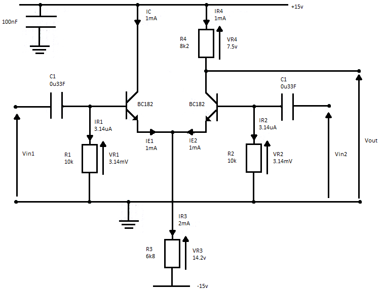
Long tailed pair circuit.png


Graphs:
View attachment frequency responses.pdf
 
Physics news on Phys.org
  • #2
What do you mean by 'offset'?

The gain is down 3dB for both the output and the RC netork. The 3dB-down frequency in both cases is about f = 100 Hz. I don't know what the value of your input capacitor C1 is but the relationship should be R1*C1 = 1/2πf, R1 = 10K (the emitter-follower input impedance is >> 10K) and therefore negligible). Have you calculated R1*C1?

I calculate the high-frequency gain (~10 KHz) to be 1mA*8.2K/26mV ~ 300 which is closer to 50dB. Why did you divide by 2 in obtaining your Gdm? If the base of Q1 goes +1 mV, the emitters go +1 mV, the base of Q2 stays at 0 mV so Vbe2 changes 1:1 with the input, not just 1/2. If I didn't miss something.
 
  • #3
Just by comparing the two graphs.. if i was to multiple the 'offset' by the rc network graph i would get the same graph as the one i measured. Yep the break should be around 100hz as that's what i designed the circuit to do. But I had to use E12 capacitors so its not exactly a 100hz but close enough.

But when you take the AC equivalent model of the left hand part of the circuit you get R1 in parallel with small rb which is equal to

rB = ([itex]\beta[/itex]+1)(re+ ze)

=[itex]\beta[/itex]re

then the sum of R1 and rb is equal to the input impedance. So its

[itex]\frac{1}{ZinC}[/itex] = ωb

C = 0.33μF and Zin = 4424Ω

where ωb = 200[itex]\pi[/itex]

as I've grounded v2 the graph I have measured is approximately equal to the differential gain of the amplifier.

Gdm = [itex]\frac{Vout}{Vin}[/itex] = [itex]\frac{Collector Current}{2 × Tail Current}[/itex] = [itex]\frac{R4}{2R3}[/itex]

I predicted this to be 164, but i do not know how this number relates to my measured graph at all.
 
Last edited:
  • #4
  • #5
Mitchy190 said:
Just by comparing the two graphs.. if i was to multiple the 'offset' by the rc network graph i would get the same graph as the one i measured. Yep the break should be around 100hz as that's what i designed the circuit to do. But I had to use E12 capacitors so its not exactly a 100hz but close enough.

But when you take the AC equivalent model of the left hand part of the circuit you get R1 in parallel with small rb which is equal to

rB = ([itex]\beta[/itex]+1)(re+ ze)

=[itex]\beta[/itex]re

then the sum of R1 and rb is equal to the input impedance. So its

[itex]\frac{1}{ZinC}[/itex] = ωb

C = 0.33μF and Zin = 4424Ω

where ωb = 200[itex]\pi[/itex]

as I've grounded v2 the graph I have measured is approximately equal to the differential gain of the amplifier.

Gdm = [itex]\frac{Vout}{Vin}[/itex] = [itex]\frac{Collector Current}{2 × Tail Current}[/itex] = [itex]\frac{R4}{2R3}[/itex]

I predicted this to be 164, but i do not know how this number relates to my measured graph at all.

No way is this circuit's cutoff frequency as dependent on β as you compute. Check your small-signal transistor model, and your analysis. R1 is practically the sole resistance in determining ω. Nobody designs circuits with a particular β in mind, and this is a pretty decent design.

What sort of capacitor is C1 again? Is it polar? That might explain why your cutoff frequency is 100 Hz instead of (1/R1*C1)/2π. You need a ceramic cap here, preferably.
 
  • #6
Thats how i worked out the value Cin though by calculating the input impedance of the circuit. And nope its not polar.
 
  • #7
Mitchy190 said:
. And nope its not polar.

Tell me the part number & make?

BTW I revised my gain calculation and it now roughly agrees with your number of 164.

How much Vin did you apply, and what did you use to measure Vout in taking your data?
 
Last edited:
  • #8
I will have to tell you that tomorrow as I am not in the lab today.

Great (:

The attachment below shows my method and measurements:
View attachment Results.pdf
 
Last edited:
  • #9
Mitchy190 said:
I will have to tell you that tomorrow as I am not in the lab today.

Great (:

The attachment below shows my method and measurements:
View attachment 53824

Gains look fine, exactly as calculated. So does your test setup.

What remains in question is your input capacitor. Disconnect the Vin1 R-C input network from the circuit and do a frequency response of the network by itself. I would bet you still get a 100 Hz 3dB rolloff.
 
  • #10
Awesome (: So how does the number 164 relate to anything? The gain changes with frequency, so I do not understand how the number 164 is equal to the differential gain. :(
 
  • #11
Mitchy190 said:
Awesome (: So how does the number 164 relate to anything? The gain changes with frequency, so I do not understand how the number 164 is equal to the differential gain. :(

You and I both calculated the gain to be about 164. We did that IN DISREGARD OF the input r-c network. Our gain calc. was based on the gain from Q1's base to the output. Mine was 8.2e3Ω*1e-3mA/(2*26mV) = 158. You used kT/q = 25 mV, I used 26 mV. So we essentially got the same answer and the data agreed with us also.

The gain changes at the low end because of your input r-c network and at the high end for several reasons including, probably, again your particular input C but also parasitic capacitances in the transistors, measuring equipment & setup, board layout, etc. etc. I still believe your input C is responsible for most of the gain variations with frequency, both at the low and high end. The midband gain around 1-3 kHz is pretty flat as it should be.

EDIT: that is why it's important you test the r-c input network stand-alone!
 
Last edited:
  • #12
Mitchy190 said:
Gdm = [itex]\frac{Vout}{Vin}[/itex] = [itex]\frac{Collector Current}{2 × Tail Current}[/itex] = [itex]\frac{R4}{2R3}[/itex]

I predicted this to be 164, but i do not know how this number relates to my measured graph at all.

I think you mean re there instead of R3

As mentioned, you are only computing the gain from the base of the transistor to the output. If you want to use the T-model this way to find the overall gain from input to output, you would ground Vin1 and write KVL from Vin1 (ground) to Vin2, remembering to replace Ib with Ie/(β+1).

But it's easier to use the half-circuit concept. You have an ac ground at the emitters (R3>>re so not much current goes through R3 and its ac voltage is therefore close to zero). So I'd keep the right side transistor, ground the emitter and find Vout/V2 where V2=(Vin2-Vin1)/2 = Vd/2

Another way to do this is find the voltage at the base of the right transistor, ie the transfer function Vb/V2. This is easy to do since you just need to move the emitter resistance to the base circuit. Then use the gain function you found already from the base. Vout/Vb. Then your overall function from input to output will be Vout/V2 = Vout/Vb * Vb/V2

If Re taken to the base side has significance compared to R2=10k, then R2 does drop the differential gain somewhat.Your calculated Gdm = 164 amounts to 20log(164) = 44dB at middle frequencies.
 
Last edited:
  • #13
Your calculated Gdm = 164 amounts to 20log(164) = 44dB at middle frequencies.

I think what the OP is saying is that the calculated gain is 44db where as the measured gain appears to be 27-28db.
 
  • #14
aralbrec said:
I think you mean re there instead of R3

I did yes sorry.

And rude man, below shows a picture of the input capacitor I used:

Capacitor.jpg


If i look at my graph where it levels out, the gain is approximately equal to 44db. Does this therefore mean my experimental value agrees with my theory? As 20log(164) = 44db?
 
  • #15
Mitchy190 said:
If i look at my graph where it levels out, the gain is approximately equal to 44db. Does this therefore mean my experimental value agrees with my theory? As 20log(164) = 44db?

Yes it does. You're separating the gain into the product of three parts: a high pass filter represented by C1/R1, a low pass filter represented by the internal capacitances of the transistor you haven't modeled and the midband gain where none of the capacitors matter.

On the high pass filter with C1 in series with the signal, notice as ω → ∞, the impedance of C1 goes to zero, meaning the input is seen unattenuated at the top of R1. So that max gain through C1/R1 is 1. Likewise with the unmodelled capacitances contribituing to the low pass filter, the max gain is 1. So these filters scale the overall response from 0 to 1, one at low frequencies and one at high frequencies. In the middle, the scaling is 1 and none of the capacitors matter.

You computed to the gain from the base of the transistor to the output by ignoring the capacitors. This means you were finding the midband gain, the gain where the low and high pass filters had no effect. So your computed gain of 44dB is what you should see at midband frequencies in your experiment.
 
  • #16
Mitchy190 said:
I did yes sorry.

And rude man, below shows a picture of the input capacitor I used:

View attachment 53866

If i look at my graph where it levels out, the gain is approximately equal to 44db. Does this therefore mean my experimental value agrees with my theory? As 20log(164) = 44db?

Yes, as I said your gain is spot-on with theory.

Did you test the r-c input network by itself as I suggested? I can't tell from the picture how good the capacitor is for this application, unfortunately.
 
  • #17
If the capacitor checks out, then I miscalculated the input impedance of the circuit (as seen at the base of Q1). I thought it was negligibly high, but if it's as low as the OP calculated then the circuit is heavily beta-dependent and thus not a good design (beta varies greatly with temperature & from transistor to transistor).

If the input resistors were changed to 1K each and the capacitors increased to 1.6uF the circuit would be a lot more stable.
 
  • #18
Summary:
1. gain computation 164 V/V from base of Q1 to collector of Q2 is correct and agrees with data.

2. Original OP compuation of input impedance (seen at Q1-b) was correct, much to my surprise. I anticipated a much higher impedance. This input impedance computed to about 5K ohms for beta = 100.

3. The circuit should be made more temperature- and device- independent by changing the input resistors to 1K and the input capacitors to around 2 uF.
 
  • #19
Okay thanks! (: how would changing those values make the circuit more stable??
 
  • #20
Mitchy190 said:
Okay thanks! (: how would changing those values make the circuit more stable??

Good question. Look at how you determined the 100 Hz cutoff frequency fc, which BTW you did correctly. Notice how important beta was? Now recalculate that frequency using beta = 200. See how much it changed fc? Now, make Rin = 1K and C = 2uF, and recalculate fc for beta = 100 and then 200. See how little fc changed now?

Basic reason: your input impedance, looking into the base of Q1, varies greatly with beta, in fact it's directly proportional to beta! And, I computed Zin ~5K ohms for beta = 100, a pretty small value. So you want the effect of this Zin to be as small as possible, and you can do that by reducing R1 to 1K from 10K. Beta for your trasistor probably has a minimum specified beta of 100 but it could easily be 200-300 for some transistors of the same type, plus it changes a lot over temperature.

If you get into this business more you will soon learn that you never design a circuit with beta-sensitive performance.

BTW if you want to trim your fc, use different-vaue capacitors but don't increase R1.
 
Last edited:

FAQ: Differential amplifer frequency responce prediction

What is a differential amplifier frequency response prediction?

A differential amplifier frequency response prediction is a mathematical model used to estimate the output voltage of a differential amplifier at different frequencies. It takes into account the input voltage, gain, and other characteristics of the amplifier to predict its performance.

Why is it important to predict the frequency response of a differential amplifier?

Predicting the frequency response of a differential amplifier is important because it helps in designing and optimizing the performance of electronic circuits. It allows engineers to identify potential issues with the amplifier and make necessary adjustments before the circuit is built.

What factors affect the frequency response of a differential amplifier?

The frequency response of a differential amplifier can be affected by various factors such as the amplifier's gain, input capacitance, load resistance, and the type of transistors used. Parasitic capacitance and inductance in the circuit can also impact the frequency response.

How is the frequency response of a differential amplifier measured?

The frequency response of a differential amplifier is typically measured by applying a small sinusoidal input signal at different frequencies and measuring the output voltage. This data is then plotted on a graph to visualize the frequency response curve.

Can the frequency response of a differential amplifier be improved?

Yes, the frequency response of a differential amplifier can be improved by using techniques such as negative feedback, choosing the right components, and minimizing parasitic effects. Simulation tools can also be used to optimize the frequency response of the amplifier.

Similar threads

Replies
4
Views
3K
Replies
6
Views
2K
Replies
2
Views
2K
Replies
6
Views
1K
Replies
11
Views
5K
Back
Top