Frequency analysis of transistor amplifiers

In summary, In summary, the conversation covers a problem involving circuit analysis and calculations for circuit (a) and (b). The calculations include determining resistor and capacitor values for specific frequencies and currents, as well as revisiting previous calculations for accuracy. The emitter bypass capacitor, Ce, plays a role in reducing negative feedback and works with the resistor Re to achieve this. However, the calculation for Ce references an internal property of the BJT, re', which is not accessible.
  • #1
Nicholas Tok
3
0
Hi guys,

I am trying to do this question on my own but i am not confident if what i am doing is correct. please download the Question2.docx file and my workings are in blue. hope someone can help me with this.

1. Homework Statement
A.
For circuit (a) below, calculate:
R_e and R_C to make I_C≈0.2 mA and V_CE≈6V.
C_e to give a pole frequency at about 400 Hz, and C_C to give a pole at about 50 Hz.

The oscilloscope input resistance is 1 MΩ. For initial calculations assume C_μ= 5pF and C_(CRO + cable)= 110 pF. (These will be measured in the lab.) The generator resistance is 50Ω, which may be taken as a good approximation to zero for this experiment. Moreover, the input will be monitored across the generator and its voltage kept constant, so it may be treated as an ideal voltage source.

Estimate the voltage gain, the frequency of the zero introduced by C_e, and the upper 3-dB frequency f_h. What is the voltage gain if C_e is omitted?
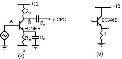
BC546B.jpg


B. Circuit (b) is to be inserted in series at point B to buffer the load capacitance. Calculate R to give a collector current of about 1.2 mA. Assuming a 'typical' value for h_fe, recalculate f_h. Is the pole frequency introduced by C_C significantly affected?

C. Leaving circuit (b) in place, a 10 kΩ resistor is inserted at point A (simulating a higher source resistance than that of the generator). Recalculate f_h. Is the pole frequency introduced by C_e affected?

The Attempt at a Solution


Question 2.docx
 

Attachments

  • Question 2.docx
    514.7 KB · Views: 344
Physics news on Phys.org
  • #2
...my workings are in blue.

?
I was not able to detect any attempt to start solving the problem.
 
  • #3
I think you should revisit the calc for Rc. It may help to label the known and desired transistor terminal voltages. Then, knowing the Collector voltage & current, you can calc Rc.

The calc for Ce shows up here as "(omega)e=1reCe", is this what was intended or is my .docx reader confused?
 
  • #4
Hi LvW,

My workings are all in the Question 2.docx it is too long winded thus I have already upload my whole questions and workings in the document file. You have download it to see my effort.
 
  • #5
Tom.G said:
I think you should revisit the calc for Rc. It may help to label the known and desired transistor terminal voltages. Then, knowing the Collector voltage & current, you can calc Rc.

The calc for Ce shows up here as "(omega)e=1reCe", is this what was intended or is my .docx reader confused?
Hi Tom,

Yes this was my attempt. Thank your for your prompt. I will look into it again.
 
  • #6
After you revisit the Rc value and the "(omega)e" equation:

Note that Re acts to introduce negative feedback in the stage, i.e. when the base voltage goes up, increasing the collector current, the emitter voltage rises due to the increased current thru Re. This rise in emitter voltage partially cancels the base voltage increase, effectively reducing the stage gain. The purpose of an emitter bypass capacitor is to avoid this emitter voltage rise; at least for a time. All these words work up to saying that the Ce value works with Re to reduce that negative feedback. Your "(omega)e" calculation references re', which is internal to the transistor and not accessible.
 
  • #7
Tom.G said:
Your "(omega)e" calculation references re', which is internal to the transistor and not accessible.

Perhaps - for a better understanding - you should realize that "re" is NOT any internal resistance. I know that, unfortunately, some authors are using such a term instead of the most important property of the BJT, which is a transconductance device: Transconductance gm=d(Ic)/d(Vbe)=Ic/Vt with re=1/gm.
As we can see, the quantity re=1/gm relates the output current change to the input voltage change - and this does not correspond to the classical definition of a resistance.
 

FAQ: Frequency analysis of transistor amplifiers

What is frequency analysis of transistor amplifiers?

Frequency analysis of transistor amplifiers is a method used to study the behavior of a transistor amplifier at different frequencies. This involves analyzing the gain, input impedance, output impedance, and frequency response of the amplifier.

Why is frequency analysis important in transistor amplifiers?

Frequency analysis is important in transistor amplifiers because it helps engineers and scientists understand how the amplifier will perform at different frequencies. This information is crucial in designing and optimizing amplifier circuits for specific applications.

How is frequency analysis performed on transistor amplifiers?

Frequency analysis can be performed using simulation software or through physical measurements. The amplifier is connected to a signal generator and an oscilloscope, and the response at different frequencies is recorded and analyzed.

What are the key parameters measured in frequency analysis of transistor amplifiers?

The key parameters measured in frequency analysis of transistor amplifiers include gain, input impedance, output impedance, and frequency response. These parameters determine the performance of the amplifier and can be used to optimize its design.

What are some common applications of frequency analysis in transistor amplifiers?

Frequency analysis is commonly used in the design and optimization of audio amplifiers, radio frequency amplifiers, and signal processing circuits. It is also used in communication systems, medical devices, and other electronic systems that require accurate frequency response.

Back
Top