Getting a High Speed Synchronous N-Channel MOSFET Driver working right

  • Thread starter techn0
  • Start date
In summary, the LTC4449 high speed n-chan mosfet driver is being used in conjunction with a 0.5a linear regulator and a 600w smps to create a 24v switching voltage. The gate driving on the bottom mosfet seems to be working properly but the gate drive on the top does not. The Schottky diode I am using is ACDBN1100-HF 100V and the boost cap is C1206C224M5UAC7800 0.22uF. I have tried several input pwm frequencies from 15k to 250k with no change. It is my understanding that a high gate singal on the top mosfet is going to
  • #1
techn0
19
5
TL;DR Summary
Need help getting high side gate working properly.
I have designed a circuit utilizing a LTC4449 high speed n-chan mosfet driver.
I am running the Vcc at 5 v from a 0.5a linear regulator 7805 type.
The switching voltage is 24v from 600w smps.
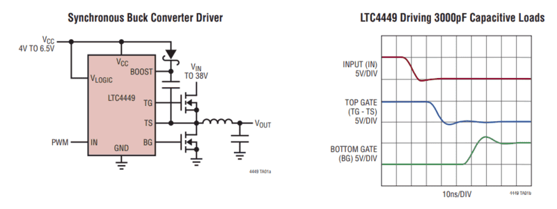
LTC4449.png

I am using this exact layout. The gate driving on the bottom mosfet seems to be working properly but the gate drive on the top does not. I think it is an issue with the boost circuitry.
The Schottky diode I am using is ACDBN1100-HF 100V
The boost cap is C1206C224M5UAC7800 0.22uF

I have tried several input pwm frequencies from 15k to 250k with no change.

It is my understanding that a high gate singal on the top mosfet is going to be 24v plus 5v. When I measure boost pin voltage it is just around 5v. Should it be 24v or 29v?

This component is a 2mm x 3mm DFN so it is ultra small and hard to work with. I have resoldiered it serveral times in an attempt to get this circuit working correctly and replaced it once. It appears to be soldered properly.

Thanks in advance for everyone's help.
 
Engineering news on Phys.org
  • #2
Welcome to PF.

I wonder if the MOSFET is turning on properly, with only 5 volts of gate drive. What make and model of MOSFET you are using?
IRF7468 ?

The boost voltage (stored in the capacitor) should be about 0.5 volt less than Vcc, measured relative to TS.
 
  • #3
techn0 said:
TL;DR Summary: Need help getting high side gate working properly.

When I measure boost pin voltage it is just around 5v.
How did you measure this? With an oscilloscope? The voltage at TS will switch between about 4.5V and 28.5V. The voltage across the capacitor will be 4 - 4.5V.

What is your switching frequency and duty cycle? Inductor, output cap, and load?

My best guess is that something isn't what you think it is. A wrong or shorted trace, a backwards diode, a 220pF cap instead of 220nF, etc. I would pause and go back and systematically verify everything, especially the stuff you think is correct. This circuit should just work.

Reread the data sheet; all of it, especially the footnotes and such.
 
Last edited:
  • #4
What about noise on the other inputs, like PWM or enable. Do you have good layout with bypass caps? Maybe it's being told to shut down when it tries to turn on?
 
  • #5
I checked voltage on both sides of the schottky diode and it is the same as the voltage of the regulator 4.95v
Here are some pictures of the signals. Running at a freq of about 125k this attempt.
Input:
InputPWM.jpg

Gates Low & High out:
OutputLow&High.jpg

As you can see there is something wrong with high side.

I have the output running through a 10uH inductor and capped with a 330uF electrolytic no load currently.

The mosfets I am using are IRF3007PBF (Data sheet says gate threshold of 2-4v)
 
  • #6
techn0 said:
The mosfets I am using are IRF3007PBF (Data sheet says gate threshold of 2-4v)
That is the threshold for conduction, Id = 250 uA.
5 volts will not really turn that MOSFET properly on.
Compare it with the 0.8 to 2.0 Gate Threshold Voltage, IRF7468, which was used by LT in the reference design.
 
  • #7
I have used this mosfet for ground switched PWM motor controllers for years with a 5v PWM signal from a PIC mcu with out a problem.
 
  • #8
techn0 said:
I have used this mosfet for ground switched PWM motor controllers for years with a 5v PWM signal from a PIC mcu with out a problem.
Maybe you were lucky.
The typical difference between the two MOSFETs is significant.
With 5 volt gate voltage, IRF7468 will sink 9 amps at 0.1 volt drop.
With 5 volt gate voltage, IRF3007 will sink 1 amp with 0.1 volt drop.
 
  • #9
Can you recommend a to-220 mosfet I should try. I will get it ordered from digikey now. I need it in that package to fit the PCB and heat sink design I have currently.

Do you think that is why the high side gate signal is wrong?
 
  • #10
You should start with the digikey parametric selection for MOSFETs, TO-220 package and low gate threshold voltage.
Then compare the datasheets.
Usually; Fig 1. Typical Output Characteristics at 25 deg C.
 
  • Like
Likes DaveE
  • #11
Possibly; STP55NF06L
 
  • #12
IRLIZ44G Do the trick?
 
  • #13
IRLIZ44G is not as good.
You will need to read the data sheets and make comparisons.
It is dawn here. I'm too tired now to make wise decisions.
 
  • #14
I ordered the one you suggested as well as a different schottky and a better plcc capacitor.
 
  • #15
techn0 said:
Do you think that is why the high side gate signal is wrong?
I think you probably have a different problem. @Baluncore is right, that MOSFET should have more gate voltage, or you should choose a MOSFET with "logic level" gate specs. But most of them should still turn on and off, just with higher resistance than you will want. Vgs(th) is between 2 - 4V for the IRF3007, you'd be unlucky to get a 4V part.

One test you could try is to lower the temperature of the device (freeze spray, ice, freezer, whatever you've got), that should lower Vgs(th). Or, you could try increasing the PS voltage to the driver as a test.

Read the data sheets yourself; all of them.
 
  • #16
I believe your main problem is the Vcc at 5 v is from a 0.5a linear regulator 7805 type. Being an emitter follower output, the high-side FET and Schottky driver cannot return reactive energy back in Vcc as a stable voltage sink. You can try a larger very-low ESR e-cap on Vcc but watch out for resonance effects and keep your probe ground short. I'd like to see textbook clean pulse waveforms and Vcc ripple < 5 mV not 1Vpp on a linear regulator.
 
  • #17
I have a 1.5a 5v smps module I could install in place of the linear regulator?
OKI-78SR-5/1.5-W36H-C

Do you think that would be a better fit for this application?
 
  • #18
Vcc error depends on impedance ratio of source to load over entire spectrum.

So that's a maybe
 
  • #19
I received the new mosfets 0.22uf Cap and Shottky Diode. I have the exact same results as before.Driver.jpg Driver solderied.jpg Curcuit.jpg

High side gate still does not work. I am so frustrated with this thing. I have re-soldered the gate driver probably a hundred times now. Only thing that changes is sometimes the low side does not work too.

I have redesigned the pcb to use this gate driver. NCP3420 because it is in a SOIC-8 package and will be loads easier to work with but it is designed for a 12v power source which is fine for running the gate IC but I still need 24 volts on the mostfets. Will I be fine running the mosfets at 24 with this gate driver? Says 35v max
 
  • #20
techn0 said:
It is my understanding that a high gate singal on the top mosfet is going to be 24v plus 5v. When I measure boost pin voltage it is just around 5v. Should it be 24v or 29v?
The boost cap will be charged to +5V, but the low voltage terminal will switch between 0V to +24V as the output MOSFETs switch. The higher voltage terminal of the boost cap will switch between +5V and +29V.

techn0 said:
I checked voltage on both sides of the schottky diode and it is the same as the voltage of the regulator 4.95v
The boost capacitor can be seen as a charge pump or a floating local power supply for the high-side gate drive.

The capacitor is referenced to the source of the high side MOSFET. That boost capacitor charges through the diode to supply voltage while the output is low. The cap then provides positive power to the high-side MOSFET gate during output high.

techn0 said:
Will I be fine running the mosfets at 24 with this gate driver? Says 35v max
Maybe we need a circuit diagram with values for the components.
I am using "Figure 4. NCP3420 Example Circuit" from the data sheet.

Vcc for the NCP3420 can be between +5V and +12V.
The positive supply to the MOSFETs, let's call it Vmm, can be higher. But (Vcc + Vmm) ≤ 35 volts, in order to meet the SW terminal absolute maximum voltage specification.
For your circuit; Vcc=5; Vmm=24; You get 29 volts which is well within spec.

Maybe the gate driver needs to be disabled by holding the OD signal low while the power supplies become stabilised, and the boost capacitor is initially charged. Only then can the high-side MOSFET be driven.

During testing, I would use a couple of 12V filament lamps in series with the 24V MOSFET supply. Select the lamp power to glow dull-red when operating, while lighting and protecting the good MOSFET, when one MOSFET fails.
 
  • #21
techn0 said:
High side gate still does not work. I am so frustrated with this thing. I have re-soldered the gate driver probably a hundred times now. Only thing that changes is sometimes the low side does not work too.
Looking at your pictures, I assume the big electrolytic capacitor is a reservoir for the 24 volt MOSFET drain circuit.

I see no bypass capacitors on the +5 volt Vcc near the gate driver. Maybe they are under the PCB?

The gate driver will not work well without sufficient fast ceramic bypass capacitance. The inductance of the tracks will be too much when Vcc must provide about one amp for fast switching of the MOSFET gate capacitance.

At high switch rates, you will need a significant Vcc supply.

I would expect a solid ground plane under the PCB, near the gate driver IC, and the lower MOSFET source.

Please provide a schematic that includes the supply bypass and reservoir capacitors.
 
  • #22
Yes the large cap is the 24v rail for the mosfets. The current pcb does not have any bypass cap near the gate driver. This is my first time using a gate driver of this sort so I did not know to use something. I will solder something in place tomorrow to give that a try. It would be miraculous if that makes this circuit work. Going to start with a 10uF ceramic unless you think some other value would be better.
 
  • #23
techn0 said:
Going to start with a 10uF ceramic unless you think some other value would be better.
A few comments;
The value of total capacitance required can be estimated from;
C=Q/V ; C = i * dt / dv; my crude guesstimates are;
i, is the average gate charge current over one cycle. 100 mA.
dv, is the allowable ripple voltage on the Vcc rail; 100 mV.
dt, is half the period of the switching; 0.5/50k = 10usec.
C = 0.1 * 10u / 0.1 = 10 uF.
That should not all be in one place, because lead inductance will reduce the value of a big lump of capacitance.
Distribute four 0u1F ceramics over the Vcc track to the ground plane, with another at the gate driver. I would use a couple of 4u7 tantalum or ceramic caps as close to the gate driver as possible.

A series resistor from the gate driver to the gate would limit the peak current and prevent possible ultrasonic oscillation. Hopefully it is not needed, my guess would be about 2V/1A = 2R2. I would lay out the PCB pads to fit a series resistor later, over a cut in a track.

You were talking of upgrading the +5 volt regulator. With sufficient distributed capacitance, that should not be necessary. Gate drive power consumption will be proportional to frequency. Check that out later if you need to PWM at greater than 50 kHz.

Make sure there is some fast capacitance close to the Vcc +5V regulator, on both input and output. As best as I can see, it looks like you got that correct in the pictures.

Tracks from the Vcc regulator to the gate driver, then to the gates, need to be wide since they are carrying one amp pulses.

The ground plane should be continuous, or run under the pulse current paths, from the Vcc reg, under the gate driver, to the lower MOSFET source. Where the ground or power passes through a via, use a patch of several vias close together, to reduce the track inductance.
 
  • #24
I ran a thicker wire from the regulator to the via near the gate driver and added a 10uF ceramic at that via. Nothing changed. High Gate still completely useless.

Here is original PCB Top traces and bottom. I do not do schematics I just draw the PCBs.
TopSide.pngBottomSide.png

Mods tried from orignal PCB are 10k PWM pull down
High current trace from reg out via to vcc via near gate driver
10uF cap placed right near gate driver
New mosfets with better low gate on specs
and of coarse resoldering and or replacing the gate driver way to many times

Nothing has improved original wave forms pictured above.

I have the bottom solder pad on the gate driver grounded. Should it not be?
 
  • #25
techn0 said:
I have the bottom solder pad on the gate driver grounded. Should it not be?
I have found no information that says the DFN8 package thermal pad is internally connected to a terminal. Since there is no connection advice, I guess it must be an electrically floating thermal pad.

You should be able to debug the PCB without the power MOSFETs installed.
 
  • #26
techn0 said:
Here is original PCB Top traces and bottom.
I cannot identify pin #1 on the NCP3420 gate driver layout.
Why are two pins tied together? Does it disable high side?
Why is the regulator ground not connected to Pgnd?

Edit: The PCB layout was for the LTC4449, not the NCP3420.
 
Last edited:
  • #27
This is an LTC4449 not NCP3420. Pin 1 is lower right
Regulator ground is connected.
Vcc and Vlogic are tied together in typical application in datasheet.
 
  • #28
I was just mentioning earlier that I have redesigned it using the mcp3420. I just sent the file off to get made today but the rest of this discussion is still me trying to get my previous iteration made with the ltc4449 working.
 
Last edited:
  • #29
I have tracking number for new PCBs so I should have an update next week.
 
  • #30
techn0 said:
... I should have an update next week.
Maybe during the wait, you can use something like LTspice to draft an updated circuit diagram.
 
  • #31
It is very difficult to even copy a good design because you don't know all the physical properties of conductors and insulators. When you combine that with a lack of understanding what to expect and lack of attention to ESR, DCR, Q, SRF Z(X(f) ZC(f), and FET Vgs vs Vt to control RdsOn and stored energy vs load energy with minor effects from Ciss, Coss for efficiency and thermodynamic properties makes your chance of success even smaller but not zero. My point is you have a lot to learn befoe you can successfully design SMPS to pass step load ringing , ripple and efficiency tests without self-destruction or NOGO. I suggest an eval kit and scope after a good SMPS simulator. There are a lot of things to learn.

The wrong inductor and pulse f and no soft start even with the right values can cause trouble.
 
  • Like
Likes cabraham
  • #32
TonyStewart said:
... makes your chance of success even smaller but not zero.
The paralysis of fear.

In any venture, all is lost if you do not take the next step.
I know that after a big step, I can always regain my balance, or jump back.

By definition, a well-designed circuit will work every time.
 
  • #33
I see things differently. If you aren't afraid to fail, go ahead . But learn the prerequisite theory of operation then the detailed acceptance criteria. You only have to meet these specs to have a perfect design. But if you don't understand the basics , how will one understand the complexities of control systems.

One of the world's best teachers now is my friend Christophe Basso who has many books on SMPS design and online help info. Formerly he was with ON Semi in France.

http://www.how2power.com/newsletters/2108/H2PToday2108_bookreview_DennisFeucht.pdf?NOREDIR=1
http://powersimtof.com/Spice.htm

There are also many books by others in [Mentor Note: links to illegal download websites deleted]
 
Last edited by a moderator:
  • #34
Baluncore said:
By definition, a well-designed circuit will work every time.
If it's on the limits and there are too many things depending on component and PCB/layout variables then it's not so sure, but prototypes and design iterations are just for that.
So (within a realistic approach) there is no need to be paralysed. If it does not work, then it'll give clues to learn from.
 
  • Like
Likes Tom.G, DaveE and Baluncore
  • #35
IMHO, Some inaccurate comments have been posted so far.

If you have an IRFxxx FET with Vt=2 to 4V , they can work well at 5V if your samples are near the 2V threshold, but this is a bad recommendation to use Vgs=5V for IRF series.
When parts are near the 4 V threshold you need 10V to compare with the spec for maxRdsOn. So the rule of Thumb is 2.5 times the max threshold voltage for minimum gate drive to be reliable. (10V/4V=2.5x) However on the sub-threshold types or "logic level FETs", this Rule of Thumb relaxes to Vgs= 2x threshold for minimum gate drive.

Also the IRFZ series is an excellent choice for logic level and the IRFZ44N is a popular low RdsOn logic level FET that "can be an excellent choice". But keep in mind RdsON * Coss = Tau tends to be constant in the same family or technology and voltage rating ,so when you choose really low Ron then it becomes a critical tradeoff with self lower resonant frequencies and losses increasing with switching rate.

Half-Bridge Dual-N Theory of Operation
1. The main requirement to work for the half-bridge with dual Nch FETs is to get the low-side PWM working to create the boost voltage needed above Vbus to greater the gate voltage for the high-side driver. check if Vgs = >=2.5 times Vt (250 uA threshold)
2. The damping losses for every part affect operation and efficiency. This means RdsOn, DCR of choke, and ESR of all caps. Too much total loop R, it falls overdamping. Too little it fails from high Q resonance, overshoot, and instability. So these are critical choices.
3. All control loops prefer 1st order feedback. This means current feedback for current error correction and voltage feedback for voltage error correction. However, the LTC4449 does not have current feedback inputs and all examples use a smart chip ahead of the drivers to take the current feedback signals to control the PWM. Without this, your dynamic performance will suffer. like step load response. Although 2nd order feedback can work with compensation to take a partial derivative of voltage feedback, it is not as good without current feedback.
4. Dead time is critical to check, so as not to cause shoot-thru currents and overheating. Too much dead-time then the flyback power duration increases. This is affected by junction temp and reactive loads. Consider 1<t< 10% of switch cycle.

these are my highlights. Good luck.

My best recommendation is follow a TI Webench design and or clone the kit layout and BOM parts. SMPS design is not trivial.

The Basso design book online is OK to use says the author to me. He welcomes the user feedback more than the publisher's revenue. This is possibly the best theory and practical book on SMPS design to date.


Also a schematic is not a "layout" of physical parts like a PCB, a schematic is a logic diagram and is missing all the parasitic analog parameters like 0.2 to 1.2 nH/mm or 0.05 to 0.5 pF stray capacitance or mutual inductance or mohms/cm resistance or ESR or DCR , decoupling caps, spectral impedance, dynamic load impedance etc .
 
Last edited:

Similar threads

Back
Top