- #1
yungman
- 5,755
- 292
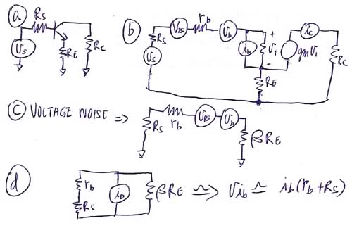
All the models I see is mostly common emitter, I have a circuit with AC equivalent shown in Fig a. Where [itex]v_s \;[/itex] is the signal voltage and the source resistance [itex]R_s[/itex]. I want to calculate the equivalent input noise voltage. Here is what I attempt to do it:
147190[/ATTACH]"]

I show the equivalent model in Fig b. I simplify by leaving the frequency depend components out for simplicity. You can see the emitter resistor and collector resistor. [itex]r_b\;[/itex] is the base resistance of the transistor. I left out output resistance to further simplify the circuit. [itex] v_{RS} [/itex] is the thermal noise of [itex] R_s[/itex] and [itex]v_b \;[/itex] is the noise voltage or the base resistance. I also left out the noise refer from the collector current back to the input by assuming gm is very high so just to look at the effect of the input components where my question is.
Fig c. show the model for calculation the equiv. input noise voltage. I assume the input resistance of the transistor is [itex]\beta R_E\;[/itex] where [itex]\beta\;[/itex] is the current gain of the transistor. As you can see [itex]\beta R_E\;[/itex] is much larger than [itex]r_b+R_s\;[/itex] therefore the input see the full [itex]v_b+v_{RS}[/itex].
Fig d is where my confusion. how do I model the input resistance. I attempt to use Fig d. but I am not sure this is correct. Can anyone verify Fig c and Fig d?
So the total noise voltage:
[tex] v_{n_{in}}=\sqrt{ v_{RS}^2 + v_b^2+v_{ib}^2}[/tex]
Thanks
Alan
147190[/ATTACH]"]
I show the equivalent model in Fig b. I simplify by leaving the frequency depend components out for simplicity. You can see the emitter resistor and collector resistor. [itex]r_b\;[/itex] is the base resistance of the transistor. I left out output resistance to further simplify the circuit. [itex] v_{RS} [/itex] is the thermal noise of [itex] R_s[/itex] and [itex]v_b \;[/itex] is the noise voltage or the base resistance. I also left out the noise refer from the collector current back to the input by assuming gm is very high so just to look at the effect of the input components where my question is.
Fig c. show the model for calculation the equiv. input noise voltage. I assume the input resistance of the transistor is [itex]\beta R_E\;[/itex] where [itex]\beta\;[/itex] is the current gain of the transistor. As you can see [itex]\beta R_E\;[/itex] is much larger than [itex]r_b+R_s\;[/itex] therefore the input see the full [itex]v_b+v_{RS}[/itex].
Fig d is where my confusion. how do I model the input resistance. I attempt to use Fig d. but I am not sure this is correct. Can anyone verify Fig c and Fig d?
So the total noise voltage:
[tex] v_{n_{in}}=\sqrt{ v_{RS}^2 + v_b^2+v_{ib}^2}[/tex]
Thanks
Alan
Attachments
Last edited:
