How Do You Design an Emitter Follower for a Stable 5V Output from a 15V Supply?

  • Thread starter dacruick
  • Start date
  • Tags
    Design
In summary: With these two conditions in mind, here are the resistor values you would need to achieve the desired voltage swing:R1 = 176 OhmsR2 = 1.8K OhmsR3 = 10K OhmsR4 = 1K OhmsIn summary, to achieve a less than 5% voltage swing with a follower with a base driven from a voltage divider, you would need to choose R1 and R2 values of 176 Ohms, 1.8K Ohms, and 10K Ohms, and R3 value of 10K Ohms.
  • #1
dacruick
1,042
1
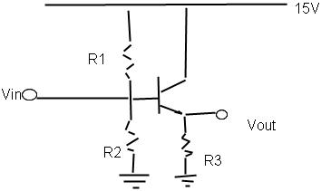
Use a follower with base driven from a voltage divider to provide a stiff source of +5 volts from an available regulated +15 volt supply. Load current (max) - 25mA. Choose your resistor values so that the output voltage doesn't drop below more than 5% under full load.
d36134dd-c9f8-44be-b4d6-fcf84b48b5d2.jpg


So I have to choose the base to be at 5 volts using R1 and R2. I'm fine with that. R2/(R1+R2) = 1/3.

Then the Emitter voltage will sit at about 4.4V. So I have to choose R3 to give 25mA when 4.4 volts are across it. That gives me 176 Ohms.

What I'm confused about is how to choose resistor values to get a less than 5% voltage swing. Someone mentioned to me that a rule of thumb is to make the current through the voltage divider 10 times the output current. But then I have R1 R2 and R3, and I don't know how to check if the voltage swing parameter is met.

Any help is greatly appreciated
 
Physics news on Phys.org
  • #2
First, if this is homework you need to identify it as such and post it in the homework section.

This problem is most easily solved by starting with the output and determining what each preceding value must be in order for the output to have the required value.

Example: If the output must be 5V, what voltage must base of the transistor have?
 
  • #3
So I have to choose the base to be at 5 volts using R1 and R2. I'm fine with that. R2/(R1+R2) = 1/3.

Are you sure about that?
What about R3?
 
  • #4
skeptic: This isn't homework, I'm just doing some exam review. The voltage at the base has to be 0.6V + 5V.studiot: R3 is a part of that voltage divider? Are you saying that it would be R2||R3 / [(R1+R2)||R3]?

And does this 5% voltage drop maximum mean that no matter what R3 is (assuming RL >> R3), the base voltage doesn't drop to more than 5.6 * 0.95?
 
Last edited:
  • #5
No I mean the voltage at the emitter = the voltage at the top (high side) of R3 = 5 volts (given).

And the voltage at the base = the voltage at the emitter + 0.6

This is the voltage to be provided by the R1 - R2 potential divider.
 
  • #6
Right, I'm fine with that. I'm saying that R2 / (R1 + R2) = 5.6V / 15V.
 
  • #7
R2 / (R1 + R2) = 5.6V / 15V.

Yes that is correct.
 
  • #8
Then I have to choose R3 so that the 15 drop across R3 gives me a maximum of 25 mA.

So now I have R3, and I need one more parameter to get values or R1 and R2. So my question is, how do I pick R1 and R2 so that the voltage swing is less than 5%. I know the ratio of R1:(R1 + R2) has to be constant, but I think the question is telling me that I can get a concise value of R1 or R2 which keeps the base voltage constant.
 
  • #9
Then I have to choose R3 so that the 15 drop across R3 gives me a maximum of 25 mA

Why?
 
  • #10
Add R4 (the load) to your circuit in parallel to R3.

should

R3>R4

or

R4>R3
 
  • #11
Well I guess if there is supposed to be a load current max of 25mA, then R4<R3 so I can get more current through R4.
 
  • #12
I have to take a break from studying because my head is about to explode. I'd really like to iron this out though. If you're not going to be around in a couple hours, would you mind just laying out the significance of this voltage swing thing for me?

I don't need much information to get this answer but you guys seem focused on slowly helping me come to the conclusion myself. Which is normally good and I understand why you're doing that, but given my time crunch I'd just really like to explicitly know where I'm wrong and what's right. This is not a homework question, it is just an exercise I saw in my readings, and I believe that I could benefit equally from the answer as I could from being lead to it.

I'm sorry about my impatience, I really am, I'm just frustrated right now and I have a buttload of stuff to learn.
 
  • #13
There are two conditions to consider.

1) Minimum (zero) current draw by the load, R4

2) Maximum current draw by the load = 25 mA.

At these conditions the output voltage will be at the extreme points (above and below) the mean 5 volts.
 
  • #14
Next you need to consider the beta or current gain of the transistor. Whatever value you choose, base current will be 1/(beta +1) of the emitter current and a change of that amount of current should not cause the base voltage to vary by more than 5%.
 
  • #15
Hmm okay. Let me try and work this out. If I make R3 quite large, can I make the approximation that when Rload is connected that no current goes through R3?

So using what skeptic has said, I have IE * 1/(Beta +1) = IB

If there is no current being drawn by RL then IE=0 and then there is no change in base voltage? If there are 25mA being drawn, then IB roughly equals 0.25mA if my Beta is 100. So that base current across R1 can't be more than 5% of 5.6 Volts?
 
  • #16
Here is a simple solution that can be refined by calculating the input resistance of the follower and using that to refine the base bias chain current.
 

Attachments

  • stiff1.jpg
    stiff1.jpg
    13 KB · Views: 842
  • Like
Likes LickMyEyeball
  • #17
Studiot said:
Here is a simple solution that can be refined by calculating the input resistance of the follower and using that to refine the base bias chain current.

Looking at this solution, I don't understand why you've chosen the currents that you have. Why is there 1 mA going through R3? Is it just arbitrary? Could you just have easily made half a mA and nothing significant changes?

The same question goes for the 2mA going through the base.

Are you saying that (R1 + R2) || (R3 + R4) would be the total input impedance? So I have to somehow use that to change R1 and R2 so that I still get 2mA?

And if everything I've said is right, I'm still not sure how to calculate the voltage swing.
 
  • #18
skeptic: This isn't homework, I'm just doing some exam review.

I still don't understand the motivation for this. No disrespect but your replies suggest limited familiarity with electronics. Are you in fact say an astronomer trying to build something for your main activity?

Right, to go through the design.

You require 25 mA through R4 at 5 volts, nominal but no less than 4.75 volts.

This has to come from the emitter current.
The balance of the emitter current flows through R3 and in particular it all flows through R3 when there is no load connected (R4 = infinity).
There is no point making this larger than necessary for waste power reasons.
Since R3 and R4 are in parallel they experience the same voltage.
A 10:1 ratio is a good rule of thumb to avoid unwanted interaction so if we choose the current in R3 to be 1/10 (approx) the current in R4 this makes it 2 mA. In fact I have chosen 1 mA to be even better in these circumstances.

Given a transistor gain (beta) of 100 that gives a base current of .26 mA at max.
By the above reasoning if we set up a standing current of 10 times this in the bias chain of R1 & R2 this would be 2.6 mA. With such a standing current drawing up to 0.26 mA will disturb the chain voltages little. I have chosen 2 mA as close enough.

The larger you make the standing current in the chain the more stable the bias voltage will be (the less effect the base current draw will have) but the more current you will be wasting heating the resistors.

So we make R1 & R2 as large as possible, commensurate with the above reasoning.

Using the 10:1 rule allows us to use the simple voltage divider formula we discussed earlier.

[tex]{V_{R2}} = \frac{{R2}}{{\left( {R1 + R2} \right)}}{V_{total}}[/tex]

If we wished to reduce the bias chain current further and increase the values of R1 & R2 we would have to take into account the fact that it is not a simple voltage divider, but R2 is shunted (in parallel with) by the input impedance of the transistor. This impedance is beta times the emitter resistance (R3 in parallel with R4) and the divider formula becomes

[tex]{V_{R2}} = \frac{{RT}}{{\left( {R1 + RT} \right)}}{V_{total}}[/tex]

where

[tex]RT = \frac{{{R_3}{R_2}}}{{{R_3} + {R_2}}}[/tex]

and of course in this case

[tex]{V_{total}} = 15[/tex]
 
Last edited:
  • Like
Likes LickMyEyeball

FAQ: How Do You Design an Emitter Follower for a Stable 5V Output from a 15V Supply?

1. What is an emitter follower design?

An emitter follower design is a common type of circuit used in electronics, particularly in amplifiers. It consists of a transistor with its emitter connected directly to the output, which follows the voltage changes of the input signal. It is also known as a common collector amplifier.

2. How does an emitter follower circuit work?

In an emitter follower circuit, the input signal is applied to the base of the transistor, which controls the amount of current flowing through the emitter to the output. The output voltage follows the input voltage, but with a smaller amplitude. This allows for voltage gain and current amplification.

3. What are the advantages of using an emitter follower design?

One of the main advantages of using an emitter follower design is that it has a high input impedance, meaning it does not load the input signal source. It also has a low output impedance, making it ideal for driving low impedance loads. Additionally, it has a voltage gain of approximately 1, providing good signal amplification without distortion.

4. What are the limitations of an emitter follower circuit?

One limitation of an emitter follower circuit is that it has a low voltage gain compared to other amplifier circuits. It also has a limited frequency response, making it unsuitable for high-frequency applications. Additionally, the output voltage may be affected by changes in temperature or variations in the transistor's characteristics.

5. How can I improve the performance of my emitter follower design?

To improve the performance of an emitter follower circuit, you can use a transistor with a higher gain, which will increase the voltage gain of the circuit. You can also use a bypass capacitor to improve the frequency response and reduce the effects of temperature and transistor variations. Additionally, using negative feedback can help improve stability and reduce distortion.

Similar threads

Replies
3
Views
2K
Replies
19
Views
4K
Replies
6
Views
3K
Replies
25
Views
8K
Replies
4
Views
3K
Replies
4
Views
2K
Back
Top