How does the tapped capacitor network increase the impedance?

In summary, The text discusses two cases where the current is conserved. In case a, the current is divided among two capacitors, which lowers the output current. In case b, the input voltage is conserved, which increases the output voltage.
  • #1
brainbaby
228
5
TL;DR Summary
Discussing increase of impedance using tapped capacitor circuit.
Please help me comprehend the text below...
Screen Shot 2019-10-27 at 10.17.28 AM.png


The discussion begins with the current flowing through the inductor for both the cases (case a and b) stays same.The input voltage is Vi. When two tapped cap is used with the current that is flowing in the inductor is divided among the two capacitor naturally lowering the output current. I assume output current to be the current across an imaginary resistor across the output terminals...Fine till here.

Now, next the text says that the input voltage Vi is conserved(i.e should be constant just like in an untapped case (a)) which increases the output voltage according to the ratio of capacitances, as the current decrease which result in an increase in impedance.

My query is from where this extra voltage comes in the circuit which tends to conserve the input voltage Vi to the same value hence increasing the impedance??
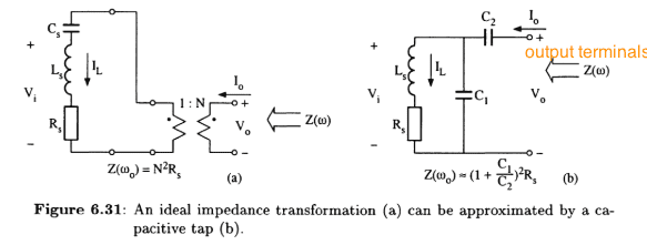
Screen Shot 2019-10-27 at 10.12.05 AM.png
 
Engineering news on Phys.org
  • #2
In diagram (b), imagine that the generator is on the "output" (RH) side, with a high resistance. Half close your eyes and you will see that C2 and C1 form a potential divider. So across C1 we have a lower resistance than the generator. There are no losses because C is reactive. Of course, by using a capacitive divider we have introduced unwanted reactance in series with our new load (R1). This is removed by L in series.
There are several ways of looking at the circuit so I will try again if you don't quite get it.
 
  • #3
Thanks for your reply.. generally a capacitive divider is just like a resistive voltage divider which also transforms the voltage i.e decrease voltage but at a specific frequency...same would have been the case here, but i am not sure about the phrase which says “increase in output voltage in accordance with the ratio of the capacitors..
I am also thinking like this that the voltage in two parrallel branches (L1 and C1) are the same...and if the voltages in both two branches are same ..then from where comes the notion that “increase in externally required voltage” comes in.
Another thing..as C1 will have lower resistance then more current should flow through it hence reducing the voltage in the C1 branch further reducing the output resistance ..but this does not support the text anyhow..
 
  • #4
tech99 said:
There are several ways of looking at the circuit so I will try again if you don't quite get it.
Alternatively, the mathematical approach would avoid the problems that are always potentially there with the 'verbal' explanation. There are very few components in the circuit so the maths wouldn't be too heavy.
 
  • #5
tech99 said:
There are several ways of looking at the circuit so I will try again if you don't quite get it.
I will appreciate if you elaborate with some more examples..
 
  • #6
brainbaby said:
I will appreciate if you elaborate with some more examples..
Or perhaps you could just look at the Maths and take it from there??
 
  • #7
I have shown how to analyse a ladder network like this, by just first placing a resistor on the right hand end and then adding each component one at a time as we work towards the left hand side. To do this we need to convert series combinations of X and R into equivalent parallel combinations, and vice versa, and I have shown how to do this.
I find it is better to use actual numbers rather than algebra, as the latter becomes very unwieldy. This way, we can keep a rough health check as we go.
I have assumed 1k resistor on the RH side and reactance values for the capacitors. The reactance of L has to provide resonance, so we find that out as we go. I end up with 8.1 Ohms on the left hand side, an impedance step up of 1000/8.1 = 123 and a voltage step up of SQRT 123 = 11.1.
 

Attachments

  • network.pdf
    482.7 KB · Views: 233
  • #8
tech99 said:
I have shown how to analyse a ladder network like this

From your example it seems that the essence of impedance matching is the series parallel conversion from where I can see that the load resistance which you have taken initially as 1k was behaving as a 100k resistance in parallel arrangement. Now as in initial post and as in the text I have talked about an increase in the externally required voltage and decrease in current increases the apparent impedance...

Two questions...
1. Is the current across LR1 branch in your figure is equal to the current across L when no tapping is used (untapped case)
and how come the text says it to be constant in both the cases?
2.Is this increase in the external voltage is the due to the increase of resistance R2' (case 2 of your fig.) from 1k to 100 k and if this external voltage increases then shouldn't the current change in the LR1 branch?
 
  • #9
brainbaby said:
My query is from where this extra voltage comes in the circuit which tends to conserve the input voltage Vi to the same value hence increasing the impedance??

The text you showed in the attached image really made me a bit confused and hard to understand.

Anyway my personal understanding is that the extra voltage, namely about the "increased external required voltage..", just refers to the voltage Vo in the output terminal.

Since the text mentions that the circuit is in certain resonant state, the impedance Z in the output terminal should be approximately resistive load to Vo. Obviously, in this case, a higher voltage value Vo should be applied to maintain the same voltages of Vi and Vs (voltage of Rs) in the circuit.

Assuming that all L and C are lossless, then (Vs^2)/Rs = (Vo^2)/Z, where Vs is the voltage of Rs in the circuit, then Z=Rs*(Vo/Vi)^2, which means that the resistance Rs is effectively increased to Z due to Vo>Vi.
 
Last edited:
  • Like
Likes brainbaby
  • #10
brainbaby said:
Two questions...
1. Is the current across LR1 branch in your figure is equal to the current across L when no tapping is used (untapped case)
and how come the text says it to be constant in both the cases?
2.Is this increase in the external voltage is the due to the increase of resistance R2' (case 2 of your fig.) from 1k to 100 k and if this external voltage increases then shouldn't the current change in the LR1 branch?
1. In the two cases, we insert the same load resistance into the LC circuit, firstly using a transformer and secondly by tapping current. So the current in L will be the same. But with zero load, the current in L is more.
2. Remember that for a series LC circuit, there is a high voltage across L and across C. This is the basis for the voltage step up.
In the attached diagram I have explained about LC matching networks.
We can match any two resistors using just L and C. But if we use two of these networks in tandem we gain a lot of flexibilty in adjustment. When we join the two LC circuits together in tandem, we usually find that two Ls or two Cs can be combined into a single component, giving three elements. So the networks using three elements are really two LC circuits in tandem. If we consider a point half way along the new ladder network, we see a resistance value that is either much higher than the two end resistors, or much lower. This is an intermediate resistance. The two LC networks work by stepping up very high, then down again, or vice versa. That is why you see a resistance value of 100k in my circuit, but only 1k and 8 Ohms at the ends.
The particular 3-element network we are studying is actually a bit difficult to analyse this way, but I have tried. In all these tee networks, the overall step up is dictated by the ratio of the end elements. The value of the centre element decides the working Q.
 

Attachments

  • network2.pdf
    244.1 KB · Views: 231
  • Like
  • Informative
Likes Tom.G and brainbaby
  • #11
alan123hk said:
Obviously, in this case, a higher voltage value Vo should be applied to maintain the same voltages of Vi and Vs (voltage of Rs) in the circuit.
Since specially at resonance the sum total of Vi and Vs is equal to Vo of the circuit. Vo is purely resistive due to resonance and since impedance is stepped up Vo will rise but if Vo rises then according tho KVL the Vi and Vs should rise to maintain the sum total of both the voltages equal to Vo, then how come Vi and Vs is maintained at same level. Please justify!

alan123hk said:
Assuming that all L and C are lossless, then (Vs^2)/Rs = (Vo^2)/Z, where Vs is the voltage of Rs in the circuit, then Z=Rs*(Vo/Vi)^2, which means that the resistance Rs is effectively increased to Z due to Vo>Vi.

Assuming no insertion losses in L and C , you have equated the power across Rs and Z as the power through inductor is neglected due to resonance...
I wonder that according to power conservation law the sum of element powers must equal zero in any circuit regardless of the elements and their component values used to construct the circuit.
So if the output resistance is increased then there must be some equal and opposite effect which it brings in the circuit to maintain the power constant.. Whats that effect??
 
  • Like
Likes alan123hk
  • #12
tech99 said:
In the attached diagram I have explained about LC matching networks.
We can match any two resistors using just L and C. B
Thanks for the explanation!
 
  • #13
brainbaby said:
Since specially at resonance the sum total of Vi and Vs is equal to Vo of the circuit. Vo is purely resistive due to resonance and since impedance is stepped up Vo will rise but if Vo rises then according tho KVL the Vi and Vs should rise to maintain the sum total of both the voltages equal to Vo, then how come Vi and Vs is maintained at same level. Please justify!

I means that Vs is the voltage across the resistor Rs, Vi is the voltage across the the serial circuit Rs and Ls.
Let the voltage across C2 is V(C2), then Vo=Vi+V(C2), so Vo is not equal to Vi+Vs.
brainbaby said:
I wonder that according to power conservation law the sum of element powers must equal zero in any circuit regardless of the elements and their component values used to construct the circuit.
So if the output resistance is increased then there must be some equal and opposite effect which it brings in the circuit to maintain the power constant.. Whats that effect??

If the entire circuit exhibits pure resistance in the output terminal, namely Z is a pure resistor, then (Vo^2)/Z becomes input power. Since there is only one lossy element Rs (also a pure resistor) in the circuit, why is V(Rs)^2/Rs not equal to (Vo^2)/Z according to the law of conservation of energy?

Anyway I indeed feel a bit confused and hard to understand about the text and the capacitive tap circuit Fig 6.31(b).

The following link shows another tapped capacitor matching circuit which is much more convincing to me.
It is also interesting that the impedance conversion formula of this tapped capacitor matching circuit has same form to that shown on Fig 6.31(b) here, Rin/RL=(1+C2/C1)^2.

https://analog.intgckts.com/impedance-matching/tapped-capacitor-matching/
 
Last edited:
  • Like
Likes brainbaby
  • #14
alan123hk said:
I means that Vs is the voltage across the resistor Rs, Vi is the voltage across the the serial circuit Rs and Ls.
Let the voltage across C2 is V(C2), then Vo=Vi+V(C2), so Vo is not equal to Vi+Vs.

If the entire circuit exhibits pure resistance in the output terminal, namely Z is a pure resistor, then (Vo^2)/Z becomes input power. Since there is only one lossy element Rs (also a pure resistor) in the circuit, why is V(Rs)^2/Rs not equal to (Vo^2)/Z according to the law of conservation of energy?

Anyway I indeed feel a bit confused and hard to understand about the text and the capacitive tap circuit Fig 6.31(b).

The following link shows another tapped capacitor matching circuit which is much more convincing to me.
It is also interesting that the impedance conversion formula of this tapped capacitor matching circuit has the formula of same form to that shown on Fig 6.31(b) here, Rin/RL=(1+C2/C1)^2.

https://analog.intgckts.com/impedance-matching/tapped-capacitor-matching/
As I mentioned, some of the three element networks are difficult to analyse, and do not fit the concept of tandem LC circuits. The link gives a good explanation of another network. Actually, it is similar to a pi network. As I mentioned, the impedance ratio of all of these is dependent on the ratio of the outer elements, and the Q is dependent on the common, or middle, element.
 
  • Like
Likes brainbaby and alan123hk
  • #15
I think that sometimes it's inevitable to involve some mathematics in order to get a clearer picture of the relevant content in engineering analysis, even though I don't like the long and tedious algebraic calculations myself.

I tried to analyze the most basic and simple tapped capacitor impedance transformer as shown below.

Tapped Capacitor Impedance Conversion.jpg
 
Last edited:
  • Like
Likes tech99 and brainbaby
  • #16
alan123hk said:
The following link shows
I need some time to conclude your inputs...I’ll get back to you once I've done..

BTW thanks for such a detailed one..
 
  • #17
Thank you alan123hk. I think this is a step down transformer, so you need an L to obtain an overall step up and also to cancel the capacitive reactance introduced by the network.
 
  • #18
tech99 said:
Thank you alan123hk. I think this is a step down transformer, so you need an L to obtain an overall step up and also to cancel the capacitive reactance introduced by the network.

Yes, that is an incomplete circuit diagram of the tap capacitor impedance transformer, which requires an L to complete the parallel resonant circuit.

After adding an L, the three elements (L,C,R) in the parallel resonant circuit are : -

1. inductor L
2 capacitor C=(C1*C2)/(C1+C2)
3 Resistor R=Z2*(1+C2/C1)^2 (In this case, let Z2 be a pure resistor)

I believe that a set of design formulas can be easily derived based on this three elements simple parallel resonant circuit, which is expected to be similar to that shown on the link above.

Interestingly, it seems that even though Z2 contains resistive and reactive components, we may still get the equivalent circuit, although the equivalent circuit would become more complicated, but I am still uncertain about that.
 
Last edited:
  • #19
alan123hk said:
Interestingly, it seems that even though Z2 contains resistive and reactive components, we may still get the equivalent circuit, although the equivalent circuit would become more complicated, but I am still uncertain about that.
The reactive part of Z2 is absorbed into C2.
 
  • #20
tech99 said:
The reactive part of Z2 is absorbed into C2

It is true that the reactive part of Z2 can be absorbed by C2 .

On the other hand, I am just curious that if Z2 contains resistive and reactive components, is the formula Z1=Z2 *(1+ C2/C1)^2 still applicable?

Therefore, I tried to simulate one example as shown below.

Tapped Capacitor Impedance Conversion 3.jpg


Based on the simulation results, the conversion still seems to be valid for frequency ranges above 300 kHz.
 
Last edited:
  • Like
Likes zoki85
  • #21
alan123hk said:
nyway I indeed feel a bit confused and hard to understand about the text and the capacitive tap circuit Fig 6.31(b).
Lets analyse fig 6.31 again...We will talk in terms of of law of conservation of power.
As law of conservation of power states that the algebraic sum of power across each component in a circuit is zero.For algebraic sum to be constant requires the individual power of all the component should be analogous to any other component , for eg. if the magnitude of the power of an individual component increase to a certain amount then there should be compensatory change by the same amount in power of another component and so forth...
So in figure 6.31a) the sum total of Power of Cs, Ls, Rs and Mutual coil is equal to constant or zero. IL in 6.31 a) is constant for two reasons:-
1. As there is no parallel path where the current IL can divide.
2.To maintain the power constant.---->Question- For power to be constant why constant current is preferred, as power depend upon other factors such as voltage and resistance as well.??

Now in second figure this current IL divides among two capacitors C1 and C2.. thus now IL decreases. Hence in 6.31b) IL changes along with output current Io.

1. Same we will take again for 6.31 a) since IL is constant in this case Vi is not changing but in 6.31 b) IL changes which further changes Vi. Now according to my bold points if Vi decreases then it should induce an equal and opposite change in any other part of the circuit to conserve the quantity which is power in this case, hence Vo (output voltage increases to an amount which is equal to the amount by which Vi decreases.
Now increase in Vo and decrease in Io can be thought of as increase in impedance ..

Hence we can say tapped capacitor increases the impedance .....BUT....
again this hypothesis brings another confusion and that is:-

2. If Vi decreases which increase Vo by same amount, should be true for the current (Io) case as well. The decrease in IL due to the capacitors, should bring an equal and opposite change in the current quantity as well so to compensate the decrease in IL the output current Io in the circuit should increase..but if Io increases then impedance should decrease which is against my conclusion 1.

Result- Both conclusion doesn't seemed to be coherent...

Please comment!
 
  • #22
  • #23
Hi Brainbaby,

Sorry, I surrender temporarily.

In fact, as I have mentioned previously, I still can't fully understand the text shown in the image on post #1, therefore, I think I may not be able to follow the reasoning method of the text to answer your question well now.

At the moment, I really don't know how to interpret the details of the circuit well in words, Maybe just give me more time, I hope I can soon give you some advice.
 
  • #24
alan123hk said:
Sorry, I surrender temporarily.

In fact, as I have mentioned previously, I still can't fully understand the text sho
Surely alan...i will be waiting for your inputs..take your own time...hopefully you would be able to interpret the text in future..

Thank you
 

1. How does a tapped capacitor network work?

A tapped capacitor network works by connecting multiple capacitors in parallel and then tapping into the network at different points. This creates multiple paths for the current to flow through, increasing the overall impedance of the network.

2. What is impedance?

Impedance is a measure of the opposition to the flow of current in an electrical circuit. It is represented by the symbol Z and is measured in ohms (Ω).

3. How does the number of capacitors in a tapped network affect impedance?

The more capacitors that are connected in parallel in a tapped network, the greater the overall impedance will be. This is because each capacitor adds its own impedance to the network, resulting in a higher total impedance.

4. How does tapping into the network at different points affect impedance?

Tapping into the network at different points allows for multiple paths for the current to flow through. This increases the overall impedance because the current has to split and flow through each path, resulting in a higher overall resistance.

5. What are the benefits of using a tapped capacitor network to increase impedance?

Using a tapped capacitor network to increase impedance can be beneficial in situations where a higher impedance is needed, such as in audio circuits or in filters. It also allows for more flexibility in designing circuits and can help reduce noise and interference.

Similar threads

  • Electrical Engineering
Replies
9
Views
1K
  • Electrical Engineering
Replies
13
Views
2K
Replies
10
Views
472
  • Electrical Engineering
Replies
8
Views
1K
Replies
4
Views
937
  • Electrical Engineering
Replies
13
Views
3K
Replies
3
Views
1K
  • Electrical Engineering
Replies
1
Views
1K
Replies
19
Views
3K
Replies
10
Views
1K
Back
Top