- 2,180
- 2,717
- Homework Statement
- N/A
- Relevant Equations
- N/A
We are currently constructing shift registers in our practicals, and I am facing an issue with the circuits. Posting this in the homework section because it arose out of college (thus, coursework).
We have to construct four types of (4-bit) shift registers — SISO, SIPO, PISO and PIPO. I feel that the circuits that are being proposed in college, though simpler than the ones I think are correct, are not actually shift registers in the strict sense of the term.
I think there are two parts to a shift register: 1. It is a register, so there should be a way to store data in it, and 2. When not storing, it should shift the stored bits either left or right. These two are required together to make a shift register. Am I correct in saying this?
We built this circuit first:

This works as long as the microprocessor is reading the data the moment it has been fed completely. (After four clock pulses, the given four bits are completely loaded into the register. But no one is stopping the clock, so the shifting will continue. The microprocessor isn't expected to keep feeding the data, and the input will subsequently go LOW after the data has been fed. Therefore, from the fifth clock pulse onwards, the stored data will be lost, unless the μC starts reading it at the fourth clock pulse.) There's no "storage" option in it.
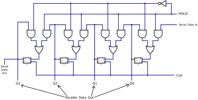
Our Prof. told us to build the controlled shift register next:

In this circuit, if I set HOLD to LOW, the output will be fed back, and thus, and the register will be able to store the fed data. This circuit, as far as I can see, works as both SISO and SIPO — if I set HOLD to LOW, it will work as storage, so I will be able to parallelly read the output lines Q3Q2Q1Q0 in this state (thus, SIPO). If I set HOLD to HIGH, the bits will shift, and I will be able to read the stored word through Q3 – thus, SISO. Am I correct in this evaluation?
Some websites, on the other hand, have given a simpler model than this:

I think, however, this will not work as SIPO in a real life scenario. My understanding is, reading the data parallelly means I can read the complete word at one go, and that cannot happen unless I store the data in some way. Yes, I can probably read the data parallelly after the fourth clock pulse (between fourth and fifth clock pulse?) when the register has the full word stored for a moment before it starts to get lost from the fifth clock pulse. But how is that even helpful? I store the data, and read it off immediately?
This is where things are starting to get messy. In our lab, we construct the clock edge with a 2-way switch + debouncer. Thus, we can control the clock. So, my classmates are contradicting me by stating that we can always decide not to supply the clock pulse, and thus, the data will be stored indefinitely even if we put the input to LOW after the fourth clock pulse. But in a real life scenario, I cannot control the clock, so I have to have feedback to store the data, and without that, I cannot read parallelly. Am I going wrong somewhere?
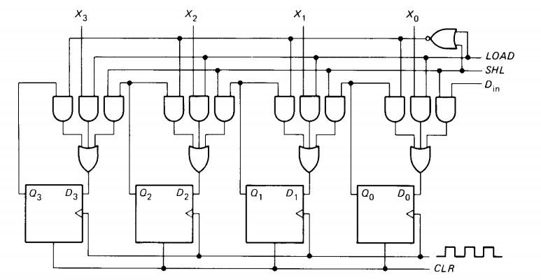
The real messy part is when parallel input comes into play. The book that we are following gives the following circuit:

Though huge, this circuit can be made to work in all the four ways (in my opinion):
This circuit is difficult to be implemented in practice using basic gates, so the following circuit was proposed in class:

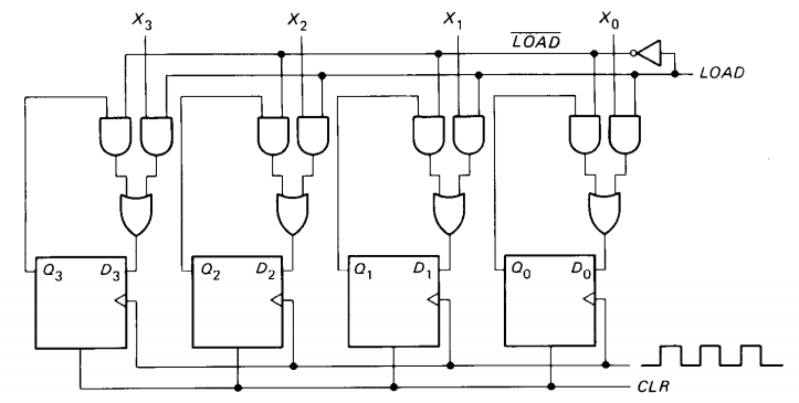
This is a buffer register and not really a shift register because there is no way the contents can shift in any direction. This is being proposed as the PIPO — parallel in, parallel out type. However, the flaw, in my opinion, is that this thing can't store. The μC will simply change the input lines once the word has been supplied to the register and one clock edge has gone (otherwise, what's the use of using a storage element?). Hence, everything that was stored will be literally lost at the next clock edge. To really store, we need a control, like the circuit below:

Here, the data will be stored if I put LOAD to LOW, and hence, parallel input (LOAD = 1) as well as parallel output (with LOAD = 0) will be possible. This can work as a PIPO register.
But serial output will not be possible.
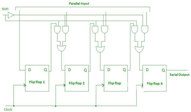
What about PISO then? For serial output, shifting is required somehow. I came across this circuit:

I don't see how this circuit will work as PISO. Yes, it can read the data parallelly with Shift = 0 and write serially with Shift = 1. But I have only two options — either shift the data, or read parallelly. There's no option to store. If I feed the data parallelly, and then put Shift to HIGH, I will have to start reading at the very next clock pulse, else I will lose data. If I feed data and then keep Shift to LOW, the data will be lost when the inputs change. Is there any option apart from the massive circuit shown above?
A really long first post, so thank you if you have come this far!
We have to construct four types of (4-bit) shift registers — SISO, SIPO, PISO and PIPO. I feel that the circuits that are being proposed in college, though simpler than the ones I think are correct, are not actually shift registers in the strict sense of the term.
I think there are two parts to a shift register: 1. It is a register, so there should be a way to store data in it, and 2. When not storing, it should shift the stored bits either left or right. These two are required together to make a shift register. Am I correct in saying this?
We built this circuit first:
This works as long as the microprocessor is reading the data the moment it has been fed completely. (After four clock pulses, the given four bits are completely loaded into the register. But no one is stopping the clock, so the shifting will continue. The microprocessor isn't expected to keep feeding the data, and the input will subsequently go LOW after the data has been fed. Therefore, from the fifth clock pulse onwards, the stored data will be lost, unless the μC starts reading it at the fourth clock pulse.) There's no "storage" option in it.
Our Prof. told us to build the controlled shift register next:
In this circuit, if I set HOLD to LOW, the output will be fed back, and thus, and the register will be able to store the fed data. This circuit, as far as I can see, works as both SISO and SIPO — if I set HOLD to LOW, it will work as storage, so I will be able to parallelly read the output lines Q3Q2Q1Q0 in this state (thus, SIPO). If I set HOLD to HIGH, the bits will shift, and I will be able to read the stored word through Q3 – thus, SISO. Am I correct in this evaluation?
Some websites, on the other hand, have given a simpler model than this:

I think, however, this will not work as SIPO in a real life scenario. My understanding is, reading the data parallelly means I can read the complete word at one go, and that cannot happen unless I store the data in some way. Yes, I can probably read the data parallelly after the fourth clock pulse (between fourth and fifth clock pulse?) when the register has the full word stored for a moment before it starts to get lost from the fifth clock pulse. But how is that even helpful? I store the data, and read it off immediately?
This is where things are starting to get messy. In our lab, we construct the clock edge with a 2-way switch + debouncer. Thus, we can control the clock. So, my classmates are contradicting me by stating that we can always decide not to supply the clock pulse, and thus, the data will be stored indefinitely even if we put the input to LOW after the fourth clock pulse. But in a real life scenario, I cannot control the clock, so I have to have feedback to store the data, and without that, I cannot read parallelly. Am I going wrong somewhere?
The real messy part is when parallel input comes into play. The book that we are following gives the following circuit:
Though huge, this circuit can be made to work in all the four ways (in my opinion):
| SHL | Mode of operation | |
|---|---|---|---|
0 | 0 | Hold / No change (⇒ parallel read possible) | |
0 | 1 | Shift left (serial out + serial in) | |
1 | 0 | Buffer register (parallel in through X's) | |
1 | 1 | Forbidden |
This circuit is difficult to be implemented in practice using basic gates, so the following circuit was proposed in class:

This is a buffer register and not really a shift register because there is no way the contents can shift in any direction. This is being proposed as the PIPO — parallel in, parallel out type. However, the flaw, in my opinion, is that this thing can't store. The μC will simply change the input lines once the word has been supplied to the register and one clock edge has gone (otherwise, what's the use of using a storage element?). Hence, everything that was stored will be literally lost at the next clock edge. To really store, we need a control, like the circuit below:
Here, the data will be stored if I put LOAD to LOW, and hence, parallel input (LOAD = 1) as well as parallel output (with LOAD = 0) will be possible. This can work as a PIPO register.
But serial output will not be possible.
What about PISO then? For serial output, shifting is required somehow. I came across this circuit:
I don't see how this circuit will work as PISO. Yes, it can read the data parallelly with Shift = 0 and write serially with Shift = 1. But I have only two options — either shift the data, or read parallelly. There's no option to store. If I feed the data parallelly, and then put Shift to HIGH, I will have to start reading at the very next clock pulse, else I will lose data. If I feed data and then keep Shift to LOW, the data will be lost when the inputs change. Is there any option apart from the massive circuit shown above?
A really long first post, so thank you if you have come this far!