Does This Circuit Compensate for Temperature-Dependent Changes in VBE?

In summary, the conversation includes discussions on temperature compensation for a circuit, specifically involving a BJT current mirror. The collector voltage of Q1 is unknown and there is uncertainty regarding the base voltage and base current. Some suggest using loop and junction rules to solve for the collector voltage, while others warn against using this type of compensation in a discrete circuit. The importance of understanding common sense design and not getting caught up in microscopic details is emphasized. The conversation also touches on the temperature coefficient of Vbe and the potential issues with using a diode to set up the Vbe for Q2. Overall, it is suggested that understanding the principles and practical applications of a circuit is more important than precise calculations.
  • #1
gnurf
370
8
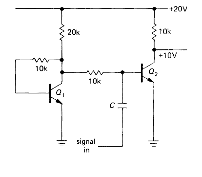
I'm trying to convince myself that the circuit below will compensate for temperature-dependent changes in VBE. But I can't seem to figure out what the collector voltage of Q1 is. Even if I assume a base voltage of 0.7V, the base current is still unknown (to me at least) so I can't calculate the drop. Can someone help a poor soul?
PqMfi.png


Edit: Just to be clear; I'm aware of the fact that the "very little" current is flowing in the 10k base resistor, and thus VC ≈ VB. I'm looking for a solution that involves less hand-waving if such a solution exists. Thanks.
 
Last edited:
Engineering news on Phys.org
  • #3
If we assume Vbe1 = Vbe1 and Ib1 = Ib2 then we can write this
Vcc - ( Ic1 + Ib1 + Ib2)*Rc1 - Ib1*Rb1 - Vbe1 = 0

And if Ic1 = Hfe * Ib

then

Vcc - ( hfe * Ib1 + 2*Ib1)*Rc1 - Ib1*Rb1 - Vbe1 = 0

And from this we can solve for Ib.

Ib = (Vcc - Vbe)/ ( Rb + (hfe + 2)*Rc1) = (20V - 0.7V)/( 10K + 102*20K) = 9.415uA

So collector voltage is equality to

Vc = Vcc - (Hfe + 2)Ib * Rc1 = 0.794V
 
Last edited:
  • #4
Thanks Jony, that makes sense!
 
  • #5
Usually people don't use 10K resistor from C to B for Q1, we just short C and B to make it a diode. But β>100 for most transistors. Assume 19.3V across the 20K resistor, current is about 1mA. Assume βa=100, base current is 10uA. So voltage drop across 10K is about 100mV. Assume Vbe of Q1 is 0.7V, implies Vce of Q1 is 0.8V or more current is diverted to the base of Q2.

With this, we know Ic of Q2 is going to be a lot higher because of the 10K. Unless Q1 and Q2 are matched pair on the same die, this is not accurate at all, Vbe between two transistor can be very different. . This is not a good practice to do current mirror at all.
 
  • #6
Hey Jony130. I was wondering how you got the following from your post above:
Jony130 said:
If we assume Vbe1 = Vbe1 and Ib1 = Ib2 then we can write this
Vcc - ( Ic1 + Ib1 + Ib2)*Rc1 - Ib1*Rb1 - Vbe1 = 0

Specifically: ( Ic1 + Ib1 + Ib2)*Rc1
I know you used loop rule on the left side of the circuit. I am assuming you used junction rule for ( Ic1 + Ib1 + Ib2) but I don't know how.

Thank you.
 
  • #7
This is nothing more then I and II Kirchoff's law and Ohms law.
attachment.php?attachmentid=50610&stc=1&d=1347199863.png


I1 = Ic1 + Ib1 + Ib2
 

Attachments

  • aa.PNG
    aa.PNG
    4 KB · Views: 1,016
  • #8
Jony130 said:
This is nothing more then I and II Kirchoff's law and Ohms law.
attachment.php?attachmentid=50610&stc=1&d=1347199863.png


I1 = Ic1 + Ib1 + Ib2
So simple, I can't believe I didn't see it. Thank you once again.
 
  • #9
gnurf said:
I'm trying to convince myself that the circuit below will compensate for temperature-dependent changes in VBE. But I can't seem to figure out what the collector voltage of Q1 is. Even if I assume a base voltage of 0.7V, the base current is still unknown (to me at least) so I can't calculate the drop. Can someone help a poor soul?

PqMfi.png


Edit: Just to be clear; I'm aware of the fact that the "very little" current is flowing in the 10k base resistor, and thus VC ≈ VB. I'm looking for a solution that involves less hand-waving if such a solution exists. Thanks.

You know that this is not a good way to do compensation? Compensation only work if the two transistors are closely coupled together. This kind of circuit only work inside IC where the two transistor are close together so temp is same and the characteristics are the same. You use discrete transistor, you can run into problem.

Also, Q1 function as a diode only to set up Vbe for Q2. If you insist on doing it like this, get rid of rb1. You are making think too complicate, way too complicate. There are ways to drown out the Vbe drift problem by using emitter resistor degeneration. Depend on what you really want, there is always a way to by pass this. If you are learning, it is more important to learn common sense design and learn ways to overcome a problem, this is neither. If it is in the IC where it is very common to use Vbe to set up current ( called current mirror) you use a diode in place of Q1.

It is not important to do exact calculation on the Ib1 and Ib2. First, β of transistor is not constant, you cannot pin down the base current. β is usually over 100 and you can assume the base current contribution is negligible. Even if you insist on all the details, it won't work as it drift with temperature, and two transistor can have very different Vbe. You are wasting time. Don't worry about it.

Again, If you want to learn calculations, first learn common sense calculation, don't get into all the detail with parameters you cannot even control. You are concentrate in the microscopic detail that you might miss the moon.
 
Last edited:
  • #10
I have the same question as gnurf. How does that circuit provide temperature compensation (assuming both transistors are the same temperature)?
 
  • #11
perplexabot said:
I have the same question as gnurf. How does that circuit provide temperature compensation (assuming both transistors are the same temperature)?

Without going deeper into math, Temp co of Vbe is about -2mV per degree C. If you have fixed bias at the base and if you don't have an emitter degenerating resistor, you will increase current with temp goes up, and further decrease the Vbe, in turn increase the current more!

The idea is if you use the diode drop across Vbe of Q1, then Q1 will provide the fixed bias that has -2mV per degree C temp coef. But as I explained, it is bad idea to do this in discrete form.

I am being very critical because I know there are good student that get good grades cannot transition into a good engineer. In school, you don't have to make the circuit work and it does not have to be cost effective, you come up with this kind of example and student actually take it to heart. This make even worst if the teacher don't work in the real world and have no idea how real life circuit design. People need to learn more common sense design rather spending a lot of time on stuff that has very little to no use in real live work.
 
  • #12
perplexabot said:
I have the same question as gnurf. How does that circuit provide temperature compensation (assuming both transistors are the same temperature)?
Without Q1 when temperature is rising Vbe2 drops. So this drop in Vbe2 causes that voltage at RB resistor increases. And this increases Ib current.
But if you add Q1 transistor to the circuit and Vbe voltage drop due to temperature rising.
This Vbe drop will increase Ib1 and Ib2 current and this increase I1 current. Which will result Vce1 voltage to drop. And this will decrease Ib1 and Ib2. So Ib2 will not increases.
Or simply this circuit provide temperature compensation because when temperature rises and Vbe drop Vce1 also drop. So the base current remain unchanged
 
Last edited:
  • Like
Likes brainbaby
  • #13
Balance the Ib1 and Ib2 is only a small part of the problem in this circuit, not to mention this is only assuming β of the two transistor track each other. Or else, you further introduce more error to the already problematic circuit. It is the Vbe that people mostly work on, β is almost always higher than 200 at 1mA tail current, error cause by Ib is negligible. Even Ib of the two transistor only cause 1% error which is same as a 1% resistor. Even inside IC, you can only count on 2% matching...at least in the days I designed IC.

You build this circuit, you'll find the Vce of Q2 can vary from +15 down to +5V easily. You breath on it and you'll see the voltage change. It is no point to even talk more about the circuit. Anyone want to start learning transistors should get the Electronics Principle by Malvino. I self studied transistor with this book 34 years ago, it is easy to understand, almost as good as explaining in English. But it give common sense approach to design. I remember the book even mention why not to design a CE stage like circuit in Q2. There are easy ways to totally bypass this problem...AND if you want precision level, use op-amp! Don't use a device that is inherently inaccurate and try to make it precision.
 
  • #14
Jony130 said:
Without Q1 when temperature is rising Vbe2 drops. So this drop in Vbe2 causes that voltage at RB resistor increases. And this increases Ib current.
But if you add Q1 transistor to the circuit and Vbe voltage drop due to temperature rising.
This Vbe drop will increase Ib1 and Ib2 current and this increase I1 current. Which will result Vce1 voltage to drop. And this will decrease Ib1 and Ib2. So Ib2 will not increases.
Or simply this circuit provide temperature compensation because when temperature rises and Vbe drop Vce1 also drop. So the base current remain unchanged
Wow, that is a very long chain of thought. It took me a while but I think I finally understand. I will review it again later on today to double check if I actually understand it. Thank you for the great explanation as always.
yungman said:
Balance the Ib1 and Ib2 is only a small part of the problem in this circuit, not to mention this is only assuming β of the two transistor track each other. Or else, you further introduce more error to the already problematic circuit. It is the Vbe that people mostly work on, β is almost always higher than 200 at 1mA tail current, error cause by Ib is negligible. Even Ib of the two transistor only cause 1% error which is same as a 1% resistor. Even inside IC, you can only count on 2% matching...at least in the days I designed IC.

You build this circuit, you'll find the Vce of Q2 can vary from +15 down to +5V easily. You breath on it and you'll see the voltage change. It is no point to even talk more about the circuit. Anyone want to start learning transistors should get the Electronics Principle by Malvino. I self studied transistor with this book 34 years ago, it is easy to understand, almost as good as explaining in English. But it give common sense approach to design. I remember the book even mention why not to design a CE stage like circuit in Q2. There are easy ways to totally bypass this problem...AND if you want precision level, use op-amp! Don't use a device that is inherently inaccurate and try to make it precision.
This is a circuit that is introducing matched biasing. I had no idea what that is, until this example. I will be studying actual current mirrors in the next section. Thank you for your valuable input. I was wondering what would happen if the two transistors had different Hfe or β, which they will undoubtedly, I guess you have confirmed my question by saying that precision will be lost greatly. I love it when I get referred to a book. I might actually pick it up. I am currently reading "The Art of Electronics," that is where I saw that circuit.
 

FAQ: Does This Circuit Compensate for Temperature-Dependent Changes in VBE?

What is a matched biasing transistor?

A matched biasing transistor is a type of transistor in which the DC biasing voltages and currents are carefully adjusted so that the transistor operates at its optimal performance level. This ensures that the transistor is operating within its specified parameters and reduces the risk of distortion or failure.

How does matched biasing affect transistor performance?

Matched biasing helps to improve the linearity and stability of the transistor, as well as reduce noise and distortion. It also helps to extend the lifespan of the transistor by preventing it from operating outside of its safe operating area.

How is matched biasing achieved?

Matched biasing is achieved by carefully selecting the appropriate values for the DC biasing voltages and currents, based on the specific characteristics and specifications of the transistor. This can be done manually or through the use of specialized circuitry or software.

What are the benefits of using matched biasing transistors?

Using matched biasing transistors can result in improved overall system performance, increased reliability and lifespan of the transistors, and reduced distortion and noise in the output signal. It also allows for more precise control and operation of the transistors.

Are there any drawbacks of using matched biasing transistors?

One potential drawback of using matched biasing transistors is that it can be more time-consuming and complex to implement, compared to using non-matched transistors. It may also require additional components and circuitry, which can increase the cost of the system. Additionally, if the biasing is not done correctly, it can lead to performance issues or even damage the transistors.

Back
Top