Mosfet failures in this differential piezo drive circuit

  • Thread starter core7916
  • Start date
  • Tags
    Mosfet
In summary: If the charge pulse and the discharge pulse gates are left floating while the 100 to 200v power is present then the gates can float to those voltages as well instantly killing the MOSFET. In summary, your switching circuit has four Mosfet that are getting bad. One of the MOSFETS is shorting between the source and drain. It is likely that this is causing the Mosfet to fail. You may need to replace one of the MOSFETs, add a fast fuse, or change the layout of your circuit to prevent this from happening.
  • #1
core7916
62
3
TL;DR Summary
why short between drain and source ?
Hello, i am using a switching circuit with the power mosfets to actuate the piezo loads, but while working on this circuit, my mosfet is getting bad, means i am observing short between mosfet source and drain. ( happend in 4 mosfets)
i will attach the circuit daigram of my circuit.
switching frequency will be 10hz with 2ms charging and rest is discharging the 3uf capacitor (ref to load and have 200kohm resistance).
in circuit c1 ref to load. and all components are rated for more than 300v. (part numbers are different in real time circuit.)
what wrong with my circuit? and what to do to avoid the shorting of mosfets.
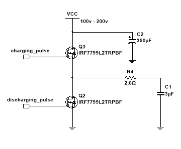
circuit.PNG
 
Engineering news on Phys.org
  • #2
Are you sure you are not overlapping the two drive signals? Maybe there is a momentary short from Vcc to ground through the two MOSFETs at the crossover points. You may need to generate your two control signals so there is a dead time between them. Can you show the full circuit with the signal generation and FET gate drive circuits?
 
  • Like
Likes Rive, DaveE and Baluncore
  • #3
When one MOSFET fails, it will probably take out the other.
A fast fuse, in the power supply or drain, may protect the second MOSFET from the first failure. That will help identify which MOSFET is failing first.

It is normal practice to include about ten ohms of series resistance in the gate drive; Rg = 10. That has two effects. It limits the switching slew rate; di/dt, and it can prevent a destructive parasitic oscillation between the driver and the MOSFET gate during switching.
 
  • Informative
Likes berkeman
  • #4
This is a 250V MOSFET in a 200V circuit. If you have ringing it would be easy to overvoltage them. OTOH, the load is well damped and turn off is benign at zero current. So I wouldn't expect much. In any case, you could try an RC snubber right at the FETs if the load is far away. But, the load is an RC snubber, so there's no point if you have good layout.

My rough calculations show that the thermal stress should be OK.

There are really only 3 ways to kill a MOSFET. Overheating, or overvoltage at the drain or gate.
 
Last edited:
  • #5
berkeman said:
Are you sure you are not overlapping the two drive signals? Maybe there is a momentary short from Vcc to ground through the two MOSFETs at the crossover points. You may need to generate your two control signals so there is a dead time between them. Can you show the full circuit with the signal generation and FET gate drive circuits?
sir, to mofets never gets on at same time since one signal is inverted input of another. and i am generating these signal from fpga controller. the controller signal will be fed to ir2110 gate driver which will drive the circuit.
 
  • #6
DaveE said:
This is a 250V MOSFET in a 200V circuit. If you have ringing it would be easy to overvoltage them. OTOH, the load is well damped and turn off is benign at zero current. So I wouldn't expect much. In any case, you could try an RC snubber right at the FETs if the load is far away. But, the load is an RC snubber, so there's no point if you have good layout.

My rough calculations show that the thermal stress should be OK.

There are really only 3 ways to kill a MOSFET. Overheating, or overvoltage at the drain or gate.
sir, the part number i have mentioned in circuit is not the same component which i ma using, i am using mosfet (STB45N40DM2AG) which has high rating (400v , 38A).
 
  • #7
core7916 said:
sir, to mofets never gets on at same time since one signal is inverted input of another
Of course they can. And if the ON FET doesn't immediately shut off while the other FET is turning ON, you have a window of vulnerability for a momentary short circuit. Do that often enough and you will heat up the FETs and cause a failure.

core7916 said:
i am generating these signal from fpga controller.
So instead of generating one signal and inverting it, generate two control signals that have a dead time (adjustable in your FPGA) between them.
 
  • Like
Likes DaveE
  • #8
The IR2110 gate driver provides independent low-side and high-side drivers. It does not prevent overlapping conduction, nor does it introduce dead time.
 
  • #9
thank you for your replies.
 
  • Like
Likes berkeman
  • #10
@core7916 -- Were you able to figure this out and get your circuit working reliably?
 
  • #11
berkeman said:
@core7916 -- Were you able to figure this out and get your circuit working reliably?
yes sir, i have kept the sufficient time between 2 signals. but this doesn't solved my issue, the actual issue is with my capacitor c2. i have replaced it, after that my circuit worked.
Thank you.
 
  • Like
Likes Tom.G
  • #12
If the charge pulse and the discharge pulse gates are left floating while the 100 to 200v power is present then the gates can float to those voltages as well instantly killing the mosfets. I have seen this on a circuit I am working with right now at only 24 volts vcc.
 
  • Like
Likes DaveE
  • #13
techn0 said:
If the charge pulse and the discharge pulse gates are left floating while the 100 to 200v power is present then the gates can float to those voltages as well instantly killing the mosfets. I have seen this on a circuit I am working with right now at only 24 volts vcc.
Yes! This is important. The gate drive circuit should always be able to source or sink current to maintain the desired voltage. Also, the Drain-Gate capacitance will act as negative feedback and couple any dv/dt at the drain back to the gate. This is dominant during switching, a huge fraction of the gate drive current flows through CDG. This is amplified in HV circuits from the Miller Effect. But there shouldn't be any DC "floating" in a healthy MOSFET, unless it comes through the other circuitry, like diode leakage and such.
 

FAQ: Mosfet failures in this differential piezo drive circuit

What causes MOSFETs to fail in a differential piezo drive circuit?

MOSFETs in a differential piezo drive circuit can fail due to several reasons, including excessive voltage or current, overheating, electrostatic discharge (ESD), and improper gate drive signals. High voltage spikes and transients can exceed the MOSFET's maximum ratings, leading to breakdown and failure.

How can overheating lead to MOSFET failure in this circuit?

Overheating can cause MOSFETs to fail by degrading the semiconductor material and other internal components. This can happen if the MOSFET is not adequately cooled, if it is operating at high power levels, or if there is poor thermal management in the circuit. Ensuring proper heat sinks, adequate ventilation, and thermal design can mitigate this risk.

What role does electrostatic discharge (ESD) play in MOSFET failures?

Electrostatic discharge (ESD) can damage the delicate gate oxide layer of MOSFETs, leading to immediate or latent failures. ESD protection measures, such as using ESD-safe workstations, grounding, and protective components like TVS diodes, can help prevent this type of damage.

How do improper gate drive signals contribute to MOSFET failure?

Improper gate drive signals, such as insufficient gate voltage, slow switching times, or excessive gate resistance, can cause MOSFETs to operate inefficiently or even enter a linear mode where they dissipate excessive power. This can lead to overheating and eventual failure. Ensuring that the gate drive circuitry is properly designed and matched to the MOSFET's requirements is crucial.

Can component mismatches in the differential piezo drive circuit lead to MOSFET failures?

Yes, component mismatches, such as using MOSFETs with different threshold voltages or switching characteristics, can lead to uneven stress distribution and failures. It is important to use matched MOSFETs and ensure that all components are compatible with the circuit's design specifications to prevent such issues.

Similar threads

Replies
1
Views
1K
Replies
1
Views
1K
Replies
5
Views
3K
Replies
1
Views
5K
Replies
33
Views
12K
Replies
5
Views
7K
Replies
5
Views
7K
Back
Top