- #1
blue2004STi
- 21
- 0
Hey all,
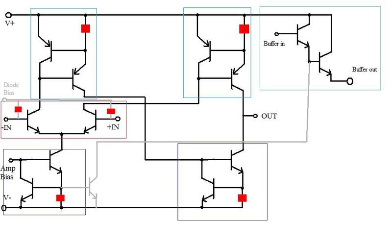
So I am a Senior in college, enrolled in a microfabrication lab. We have a final project to do and we're already being asked to come up with all of the design and physical sizes along with beginning simulations. The reason is so we will for sure have everyone's design by the time we have to start fabrication. Well I chose to model after a operational transconductance amplifier that I'm using for a different project. The background for this class is basically I have to implement everything in pMOS. Our professor has outlawed nMOS, bipolar, diodes, and the like. Now I'm looking over the equivalent circuit and I'm having trouble understanding a few things. I drew up a circuit diagram(yes in MS paint, I'm in a lab that doesn't have one single circuit schematic program).

The black portions are still in BJT as of yet and are what I believe I need to keep. The grey stuff is what I am omitting, but is there to show other connections that may be relevant and the filled red squares are where diodes used to be. So I understand that the red boxed area is a BJT differential input and I obviously the green boxed area is a simple BJT buffer amp. My problem lies with the light blue and purple boxed areas. I can see that they are similar except the purple are npn where the light blue are pnp, so my first thought was "CBJT"(?)lol but that didn't fit in my head. So I thought maybe it's an active load used as a pull up/ pull down network but once again that doesn't seem to fit. I know that there has to be a high gain stage, but contrary to what my professor said I don't see how these are in a cascode configuration. I'm really lost right now. Any thoughts would be helpful.
Thanks,
Matt
So I am a Senior in college, enrolled in a microfabrication lab. We have a final project to do and we're already being asked to come up with all of the design and physical sizes along with beginning simulations. The reason is so we will for sure have everyone's design by the time we have to start fabrication. Well I chose to model after a operational transconductance amplifier that I'm using for a different project. The background for this class is basically I have to implement everything in pMOS. Our professor has outlawed nMOS, bipolar, diodes, and the like. Now I'm looking over the equivalent circuit and I'm having trouble understanding a few things. I drew up a circuit diagram(yes in MS paint, I'm in a lab that doesn't have one single circuit schematic program).
The black portions are still in BJT as of yet and are what I believe I need to keep. The grey stuff is what I am omitting, but is there to show other connections that may be relevant and the filled red squares are where diodes used to be. So I understand that the red boxed area is a BJT differential input and I obviously the green boxed area is a simple BJT buffer amp. My problem lies with the light blue and purple boxed areas. I can see that they are similar except the purple are npn where the light blue are pnp, so my first thought was "CBJT"(?)lol but that didn't fit in my head. So I thought maybe it's an active load used as a pull up/ pull down network but once again that doesn't seem to fit. I know that there has to be a high gain stage, but contrary to what my professor said I don't see how these are in a cascode configuration. I'm really lost right now. Any thoughts would be helpful.
Thanks,
Matt
Last edited: