Optimal thin absorber of electromagnetic energy

  • #1
Leo2024
1
0
Hi, I am a material engineer and have a question about a formula derivation relative to microwave absorption. I really cannot figure it out after days of trying. This should be simple for a specialist.

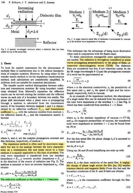
In this attached paper, how could one derive Eq(10) based on Eq (8) and (9)? Is k_2 in Eq (8) a complex number?
screenshot.jpg

Source: https://www.researchgate.net/profil...of-the-permeable-base-transistor.pdf#page=168
 
Engineering news on Phys.org
  • #2
Thread closed temporarily for Moderation...
 
  • #3
Thread is reopened provisionally...
 
  • #4
I read eq. (9), and its surrounding text, as saying that the complex part is so small that that it can be ignored - leading to eq. (10) being real (with the complex part negligible).

Caveat: Not an expert in the field, just my interpretation of the text and equations.

Cheers,
Tom
 
  • #5
Leo2024 said:
In this attached paper, how could one derive Eq(10) based on Eq (8) and (9)? Is k_2 in Eq (8) a complex number?
You can rewrite eq.(8) of the paper in the form:$$Z_{1-2}\left(d\right)=\eta_{0}\left(\frac{\eta_{\mathrm{met}}}{\eta_{0}}\right)\left(\frac{1-j\left(\frac{\eta_{\mathrm{met}}}{\eta_{0}}\right)\tan\left(k_{2}d\right)}{\left(\frac{\eta_{\mathrm{met}}}{\eta_{0}}\right)-j\tan\left(k_{2}d\right)}\right)\tag{1}$$You already know from eq.(9) that ##\left|k_{2}d\right|\ll1##, but it's also true that ##\left|\eta_{\mathrm{met}}/\eta_{0}\right|\ll1## because the impedance of a good-conducting metal is very small. So we can expand (1) to lowest order in the two small quantities to get:$$Z_{1-2}\left(d\right)\approx\frac{\eta_{0}\left(\frac{\eta_{\mathrm{met}}}{\eta_{0}}\right)}{\left(\frac{\eta_{\mathrm{met}}}{\eta_{0}}\right)-jk_{2}d}=\frac{\eta_{0}\,\eta_{\mathrm{met}}}{\eta_{\mathrm{met}}-j\eta_{0}\,k_{2}d}\tag{2}$$Now rewrite eq.(6) and the definition of impedance, in terms of the metal's conductivity ##\sigma_{\mathrm{met}}## and skin-depth ##\delta_{s}\equiv\sqrt{\frac{2}{\omega\mu\sigma_{\mathrm{met}}}}##:$$k_{2}=\frac{1+j}{\delta_{s}},\;\eta_{\mathrm{met}}\equiv\frac{\omega\mu}{k_{2}}=\frac{1-j}{\sigma_{\mathrm{met}}\,\delta_{s}}\tag{3a,b}$$Finally, insert this into (2) to yield:$$Z_{1-2}\left(d\right)\approx\frac{\eta_{0}}{1+\eta_{0}\,\sigma_{\mathrm{met}}d}=\frac{R_{S}\,\eta_{0}}{R_{S}+\eta_{0}}\tag{4}$$where ##R_{S}\equiv1/\left(\sigma_{\mathrm{met}}d\right)##.

(Edited to include absolute-value signs in the inequalities.)
 
Last edited:
  • Like
Likes Leo2024 and Delta Prime

FAQ: Optimal thin absorber of electromagnetic energy

What is an optimal thin absorber of electromagnetic energy?

An optimal thin absorber of electromagnetic energy is a material or structure designed to maximize the absorption of electromagnetic waves, such as light, while minimizing reflection and transmission. These absorbers are typically engineered to have specific properties that allow them to efficiently convert incident electromagnetic energy into other forms of energy, such as heat, over a desired range of wavelengths.

How does the design of an optimal thin absorber work?

The design of an optimal thin absorber often involves the use of metamaterials, which are engineered to exhibit unique electromagnetic properties not found in nature. By manipulating parameters such as thickness, material composition, and surface structure, these absorbers can be tuned to resonate at particular frequencies, enhancing their absorption capabilities. Techniques such as impedance matching and the use of resonant structures are commonly employed to achieve optimal performance.

What are the applications of optimal thin absorbers?

Optimal thin absorbers have a wide range of applications, including in photovoltaics (solar cells), thermal emitters, sensors, and stealth technology. In photovoltaics, they can enhance light absorption to improve energy conversion efficiency. In thermal emitters, they can be used to design devices that emit thermal radiation at specific wavelengths. Additionally, in stealth technology, they can help reduce the radar signature of objects by absorbing electromagnetic waves.

What materials are commonly used in optimal thin absorbers?

Common materials used in optimal thin absorbers include metals, semiconductors, and dielectrics. Metals like gold and silver are often used due to their plasmonic properties, which can enhance absorption at certain wavelengths. Semiconductors can be engineered to have specific bandgaps, allowing for tailored absorption characteristics. Dielectric materials are also used, particularly in multilayer structures, to create interference effects that enhance absorption across a range of frequencies.

What are the challenges in creating optimal thin absorbers?

Creating optimal thin absorbers presents several challenges, including achieving broad spectral absorption, minimizing losses, and maintaining structural stability. Balancing the trade-off between absorption efficiency and bandwidth can be difficult, especially when working with thin films. Additionally, the fabrication of complex structures at the nanoscale can be technically demanding and costly. Researchers are continually exploring new materials and fabrication techniques to overcome these challenges and improve the performance of absorbers.

Back
Top