Small Signal Input Resistance of a BJT amplifier

In summary: For the realisation of a precise emitter follower (or any other type of amplifier) - one has to take into account temperature, supply voltage variations, and parameter spreads of the transistors.(3) In the case of an emitter follower it is common to use the thermal feedback of the transistor to stabilize the temperature and the DC quiescent point.(4) In the case of an emitter follower it is common to use the emitter resistor RE to stabilize the DC quiescent point and to provide a certain DC feedback. Hereby the DC feedback is related to the DC emitter voltage and the DC collector current.(5) In the case of an emitter follower it is common to use
  • #1
anvoice
16
3
Homework Statement
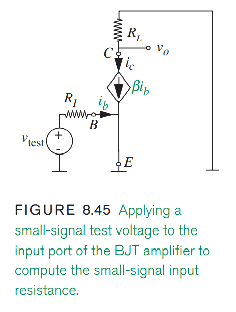
Find the small signal input resistance to a BJT amplifier.
Relevant Equations
iB = Vtest / Rinput
iC = beta x iB
The diagram of the BJT amplifier small signal model is below. This is not really a homework question as I am self-learning electronics, but I was advised it may be better placed here than in the technical portion of the forum. Thus I do not have an "attempt" at a solution (which is given as RI or Rinput by the text example), but rather some ruminations as to why the answer is what it is. I understand that generally, the input resistance in the presence of dependent sources can be measured as a ratio of Vtest to the produced current. However, I do not understand why we measure only the current iB (which is Vtest / Rinput according to Ohm's law) versus either iC (which is beta x iB per the constituent relation) or iE (which is iB + iC). That is, what is the strict definition of the "produced current" in this case? Since there are multiple currents generated by the voltage Vtest, why is it that only the one through the input resistor branch matters? Thanks in advance!
BJT_Amp.png
 
  • Like
Likes Delta2
Physics news on Phys.org
  • #2
Consider an emitter-follower.
For a small signal, the voltage on the emitter, follows the voltage on the base.
But the base current is; Ib = Ie / β ; So the input resistance is β * Re .
Take a look at https://en.wikipedia.org/wiki/Common_collector
 
  • #3
anvoice said:
Homework Statement:: Find the small signal input resistance to a BJT amplifier.
Relevant Equations:: iB = Vtest / Rinput
iC = beta x iB

I do not understand why we measure only the current iB
This is simply the definition of "input resistance". Yes, there are other things to measure too, but they would be called something else. Input resistance is always the input voltage divided by the input current, that is all. If you want to learn more you could look into "h-parameters" or "Z-parameters" of transistors or networks.
 
  • #4
anvoice said:
Homework Statement:: Find the small signal input resistance to a BJT amplifier.
Relevant Equations:: iB = Vtest / Rinput
iC = beta x iB

why is it that only the one through the input resistor branch matters?
While the previous answers were more accurate and detailed, one way of interpreting the circuit you supplied is:
To a first level of approximation all wires have Zero resistance, therefor the "B" terminal is directly connected to VTEST minus.

That works for this particular diagram because the intrinsic resistance of the Emitter is ignored. As you get to more detailed analyses, the Emitter resistance shows up just above, and in series with, the "E" terminal.

Hope this helps!
Cheers,
Tom
 
  • #5
Baluncore said:
Consider an emitter-follower.
For a small signal, the voltage on the emitter, follows the voltage on the base.
But the base current is; Ib = Ie / β ; So the input resistance is β * Re .
Take a look at https://en.wikipedia.org/wiki/Common_collector
Thanks, I'll be reading through that.
DaveE said:
This is simply the definition of "input resistance"... If you want to learn more you could look into "h-parameters" or "Z-parameters" of transistors or networks.
Big thanks, I will take a look at those. I see one definition of "input resistance" as the resistance seen by the current source or voltage source which drives the circuit. Unfortunately I don't see a good definition of "seen" here, nor do I understand why it has to be specifically the current through the input resistance when there are other currents in play before the input current manages to complete the loop (that is, iC combines with iB to make iE). Still confused sadly.
Tom.G said:
While the previous answers were more accurate and detailed, one way of interpreting the circuit you supplied is:
To a first level of approximation all wires have Zero resistance, therefor the "B" terminal is directly connected to VTEST minus.

That works for this particular diagram because the intrinsic resistance of the Emitter is ignored. As you get to more detailed analyses, the Emitter resistance shows up just above, and in series with, the "E" terminal.

Hope this helps!
Cheers,
Tom
Right, the current up to the emitter is certainly iB. However, past there and to complete the loop to the test voltage source, it becomes iE... So I'm still not sure why it's just iB that we account for.

Just want to say I really appreciate all the advice so far. I think what I'm struggling with most is a definition of "input resistance" that makes sense to me.
 
  • #6
Baluncore said:
Consider an emitter-follower.
For a small signal, the voltage on the emitter, follows the voltage on the base.
But the base current is; Ib = Ie / β ; So the input resistance is β * Re .
Take a look at https://en.wikipedia.org/wiki/Common_collector
The expression β * Re is a rather rough approximation ...what happens for RE=0 (as in the question)?
In this case (RE=0), the remaining resistance is the small-signal resistance between base and emitter (rbe).
For calculating this resistance rbe we use the definition:

rbe=d(Vbe)/d(Ib) which also can be written as
rbe=[d(Vbe)/d((Ic)]*[d(Ic)/d(Ib)]=(1/g)*β=β/g

with β=small signal current gain and
g=transconductance=Ic/Vt

(transconductance g depends directly on the DC collector current Ic and the temperature voltage Vt=26mV (room temperature)

Example: β=100, Vt=25mV, Ic=1mA
rbe=100*25=2.5kOhm
 
Last edited:
  • #7
LvW said:
The expression β * Re is a rather rough approximation ...what happens for RE=0 (as in the question)?
Considering the case of an emitter-follower, the resistance Re would not be zero, and
β * Re would be a first approximation. But it is easy to understand.

As a small-signal amplifier, the OP schematic, fig 8.45, is too rough, with gain being totally dependent on the wide spread of parameter β. That is not the case with an amplifier having an emitter resistor, Re, such as an emitter-follower.
 
  • #8
Baluncore said:
Considering the case of an emitter-follower, the resistance Re would not be zero, and
β * Re would be a first approximation. But it is easy to understand.

As a small-signal amplifier, the OP schematic, fig 8.45, is too rough, with gain being totally dependent on the wide spread of parameter β. That is not the case with an amplifier having an emitter resistor, Re, such as an emitter-follower.
(1) OK - I fully agree that for an emitter follower with β*RE>>rbe the approximation r_in=β*RE might be sufficient.
However, for my opinion it is essentiell for an engineer to KNOW about the simplifications/approximations he has made - and under which restrictions such an approximation is OK.
And I think, also a newbie should learn from the beginning how to handle such approximations.
Therefore, even for beginners, I think it would be helpful to mention the complete expression
r_in=rbe+β*RE
which can be used for all values of RE (including zero). And it clearly shows when the value of rbe plays a minor role.

(2) More than that, from the original question I understood that the questioner is a beginner and wants to know something about the definition and the meaning of the BJT`s input resistance at the base.
For my understanding, he was not asking if it is a good working circuit with a stable Ic (less sensitive to β variations.
His circuit shows the emitter grounded (RE=0) and not an emitter follower.
This was the basis of my answer.
 
Last edited:
  • #9
LvW said:
This was the basis of my answer.
You objected to my answer. I did not object to yours.
The reader has sufficient intelligence to read and understand both.
If you want me to delete or withdraw my answer, you should report my post.
 
  • #10
Baluncore said:
You objected to my answer. I did not object to yours.
The reader has sufficient intelligence to read and understand both.
If you want me to delete or withdraw my answer, you should report my post.
Sorry, if you had the impression that I have "objected" your answer.
For my opinion, I only have mentioned that (a) it was an approximation and (b) that it did not reflect the case RE=0 (as shown in the diagram).
What would YOU do in such a case (when you have the feeling that a mentioned formula is an approximation only)?
 
  • #11
LvW said:
What would YOU do in such a case (when you have the feeling that a mentioned formula is an approximation only)?
Life is an approximation. Engineering is an approximation.
I would post my answer, then walk away and avoid wasting my time messing up the thread.
 
  • #12
Baluncore said:
Life is an approximation. Engineering is an approximation.
I would post my answer, then walk away and avoid wasting my time messing up the thread.
OK - that`s what you can do when you are the first to answer (as in this case).
But I came after you and - for my feeling - it could be helpful for the questioner (who is a beginner) to point to the fact that a formula (given in a previuos answer) is an pretty rough approximation (even without mentioning this fact).
I think, such an additional explanation should be allowed in this forum for beginners.
 
  • #13
LvW said:
I think, such an additional explanation should be allowed in this forum for beginners.
You gave the additional explanation, and I would have left it if you had not asked this direct question.
LvW said:
The expression β * Re is a rather rough approximation ...what happens for RE=0 (as in the question)?
What is it with you. Get over it.
 
  • #14
OK - I will follow your advice.
 
  • Like
Likes Delta2
  • #15
Thank you to everyone who tried to help. I understand that the diagram might not detail a typically used circuit, its virtue is simplicity so I was hoping to at least understand that. I will definitely try to understand the common emitter fully, along with the approximations made, when I come to it.

It seems though that I am missing something fundamental. If the input resistance is the "resistance seen by the current source or voltage source which drives the circuit" (is that right?), then don't we need to choose two points at least to observe the said resistance (e.g. between the + and - terminals of the test voltage source in the diagram)? Since currents flow in loops (and through branches), and voltages are observed between two points? Then, why do we have to choose specifically the branch connected directly to the positive terminal of the test voltage, observe its current before it joins the collector current to form the emitter current, and conclude that the input resistance "seen" by the voltage source is just RI (Rinput)? Sorry if I'm rephrasing previous statements, but I just don't understand the concept with the information previously given here or in the text.
 
  • #16
anvoice said:
It seems though that I am missing something fundamental. If the input resistance is the "resistance seen by the current source or voltage source which drives the circuit" (is that right?), then don't we need to choose two points at least to observe the said resistance (e.g. between the + and - terminals of the test voltage source in the diagram)?
Correct. The input current or voltage source is referenced to ground, common, or earth.

A voltage source is assumed to have zero resistance, while a current source has infinite resistance.
 
  • #17
Hi again @anvoice,

"Input Resistance" should perhaps be called "Equivalent Input Resistance."

Renaming it with "Equivalent" points out that, if instead of connecting VTEST to the transistor you connect a resistor of the same value across VTEST, then the voltage and the current of VTEST will be the same as if the transistor were connected there.

And yes, the various currents in a transistor DO interact, and that is what the equations above that include β show. Those equations are the next step of complexity to more accurately understand/describe the circuit.

Another fine-point definition: Input Resistance is what any Source connected to an input (of any device) reacts to as a load. If the source is a Voltage source, then as the resistance goes up the current goes down. It doesn't matter if the load is a resistor, diode, or transistor...
... (well -- almost doesn't matter, see the previous paragraph. Diodes and transistors change their apparent resistance depending on how much current is flowing thru each of their pins; that is another way of saying that they are nonlinear devices. But that is another can-of-worms, for much later!)

Hang in there, at some point that light bulb in your head will light up. 😁

Cheers,
Tom
 
  • Like
Likes anvoice
  • #18
Tom.G said:
Hang in there, at some point that light bulb in your head will light up. 😁
Thanks Tom, I'm counting on it! Let's hope the resistance on that is not too high. :biggrin:

Baluncore said:
Correct. The input current or voltage source is referenced to ground, common, or earth.
That's what's confusing me in the example then. As the current iB from the + input splits, depending on which way you turn to get to ground, the current becomes either -iC or iE. So why are we justified in stopping at the base of the BJT and saying "this is the input current"?
 
  • #19
anvoice said:
As the current iB from the + input splits, depending on which way you turn to get to ground, the current becomes either -iC or iE.
Not quite. The Collector junction is reverse biased so the Base current can't go that way, it flows out the Emitter.

Anyhow, we are talking about the Base as the input, so it doesn't really matter where the current flows after it gets in the transistor. All we need is to know how much current is entering the Base so we can determine the effect on the source voltage, VTEST in the present circuit.

(By the way, just to complicate matters, the circuit as shown would typically be a simplified circuit for finding the AC characteristics of the stage and its loading of the signal source (prior stage).)

Cheers,
Tom
 
  • #20
anvoice said:
That's what's confusing me in the example then. As the current iB from the + input splits, depending on which way you turn to get to ground, the current becomes either -iC or iE. So why are we justified in stopping at the base of the BJT and saying "this is the input current"?

Just to avoid misunderstanding on your side:
As far as I can see, up to now we only spoke about the input resistance at the base node.
With respect to the circuit as shown in your first post, there is an external ohmic resistor between the input source and the base node. Of course, when you are interested in the input resistance of the whole circuit this resistor must be added to the resistor which does exist (can be measured resp. computed) at the base node.
 
  • #21
Tom.G said:
Not quite. The Collector junction is reverse biased so the Base current can't go that way, it flows out the Emitter.

Anyhow, we are talking about the Base as the input, so it doesn't really matter where the current flows after it gets in the transistor.
Ok, I think it's clearing up. I was looking at the subcircuit without considering it as a complete device and that might have confused me. So our input resistance is literally just the resistance it takes to get to (and through, assuming a nonzero base resistance) the base of the transistor?
LvW said:
Just to avoid misunderstanding on your side:
As far as I can see, up to now we only spoke about the input resistance at the base node.
With respect to the circuit as shown in your first post, there is an external ohmic resistor between the input source and the base node. Of course, when you are interested in the input resistance of the whole circuit this resistor must be added to the resistor which does exist (can be measured resp. computed) at the base node.
Yes, I was always thinking about the circuit with that in mind. The external ohmic resistor is what determines the resistance in this case because the resistance of the base itself is theoretically zero (or otherwise really small) if I now understand correctly. I never really thought about it without the context of an input resistor since that usually makes BJT transistors burn up.

Curiously enough and a bit out of context, I once ran into a situation where putting too small a resistor on the gate of a MOSFET (not BJT) and attempting to forward bias it burned (literally) the MOSFET. Interesting because we usually think about the input resistance of a MOSFET as infinite, but that's probably also an approximation.

Cheers everyone, you've been a great help!
 
  • #22
anvoice said:
"Yes, I was always thinking about the circuit with that in mind. The external ohmic resistor is what determines the resistance in this case because the resistance of the base itself is theoretically zero (or otherwise really small) if I now understand correctly."
Oh no - that's not correct!
The input resistance at the base node can be several kOhms (when the emitter is ac-grounded) and can be much larger when there is an ac-effective emitter resistor (negative feedback effect).
In my post'6 I gave you an example.
 
  • #23
LvW said:
Oh no - that's not correct!
The input resistance at the base node can be several kOhms (when the emitter is ac-grounded) and can be much larger when there is an ac-effective emitter resistor (negative feedback effect).
In my post'6 I gave you an example.
Ah, I see. I'll need to keep reading to understand that formula properly. Thanks a bunch!
 
  • #24
anvoice said:
Ah, I see. I'll need to keep reading to understand that formula properly. Thanks a bunch!
Understanding the way components behave, and learning what mathematics best describes them, are two different things that should be grown together.

I believe the problems in this thread began when the confusing schematic was chosen in the OP.

I would suggest that the first approximation of the common-collector emitter-follower should be chosen for the first venture into the field of BJT input and output impedance.
 
  • Like
Likes Tom.G

FAQ: Small Signal Input Resistance of a BJT amplifier

What is the definition of small signal input resistance of a BJT amplifier?

The small signal input resistance of a BJT amplifier is a measure of the resistance seen by the input signal at the base of the transistor. It is the ratio of the change in input voltage to the resulting change in input current, assuming the output voltage and current remain constant.

How is the small signal input resistance calculated?

The small signal input resistance can be calculated by dividing the change in input voltage (ΔVin) by the change in input current (ΔIin). This can be expressed as Rin = ΔVin/ΔIin.

What factors affect the small signal input resistance of a BJT amplifier?

The small signal input resistance of a BJT amplifier is affected by the biasing of the transistor, the load resistance, and the internal resistance of the transistor itself. It also depends on the frequency of the input signal, as well as the physical characteristics of the transistor such as its size and doping levels.

How does the small signal input resistance impact the performance of a BJT amplifier?

The small signal input resistance is an important parameter in determining the gain and stability of a BJT amplifier. A high input resistance allows for a larger input signal to be applied without significantly affecting the output signal, resulting in a higher gain. A low input resistance can cause instability and distortion in the output signal.

How can the small signal input resistance be improved in a BJT amplifier?

The small signal input resistance can be improved by using a larger load resistance, which decreases the effect of the internal resistance of the transistor. It can also be improved by using a larger transistor with lower internal resistance, or by using a biasing circuit that increases the input impedance. Additionally, using negative feedback can also improve the small signal input resistance of a BJT amplifier.

Similar threads

Replies
8
Views
2K
Replies
18
Views
3K
Replies
2
Views
3K
Replies
9
Views
2K
Replies
12
Views
2K
Replies
1
Views
1K
Replies
4
Views
3K
Replies
4
Views
2K
Replies
2
Views
2K
Back
Top