VHF Tuner Circuit: Matching 75Ω Impedance with Tapped Coil

  • Thread starter brainbaby
  • Start date
  • Tags
    Circuit
In summary, the circuit is a VHF front-end that is used for wide-band TV reception. It has an auto transformer formed by the tapped coil. The turns ratio is N and the square root of the impedance ratio is found. The equivalent series resistance of the coil is found and the reactance of the 15pF shunt capacitor is found. The loaded Q of the 15pF shunt capacitor is found. The parallel equivalent across the 15pF shunt capacitor is found.
  • #1
brainbaby
228
5
Hi friends,

I want to frame out how 75Ω impedance is matched by using tapped coil and two shunt capacitors connected in parallel. I think so for that I have to calculate the load value, and if we take the entire circuit out to be as a load then the most acute hurdle would to be to calculate the load value of the circuit.
I am completely messed up ..please help..??

Thanks
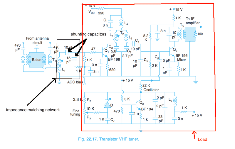
Screen Shot 2016-11-14 at 8.47.32 am.png
 
Engineering news on Phys.org
  • #2
The 75 ohms is matched by the tap low down on L1. The top of L1 is much higher impedance.
As shunting capacitors, the 10pF in series with 15pF will peak resonance of L1 in VHF band. They then form a capacitive voltage divider that applies RF to the base of Q1.

You should think of the 10 pF as the top of a Pi matching network, with L1 and the 15pF as the two legs. That network matches the high impedance of L1 to the base of Q1.
 
  • Like
Likes brainbaby
  • #3
Baluncore said:
They then form a capacitive voltage divider that applies RF to the base of Q1.

If you are talking about resonance as what every tuner circuit meant out to be ...then how can we think of that the capacitors would divide voltages...
At resonance the imaginary part of the impedance of coil L1 and capacitors ( 10pf and 15 pf) will cancels each other resulting no current to flow across it causing the voltage from antenna side to perfectly couple to the base of Q1...hence they shouldn't acts as a voltage divider...

also...
please elaborate...
Baluncore said:
The top of L1 is much higher impedance.
 
  • #4
brainbaby said:
At resonance the imaginary part of the impedance of coil L1 and capacitors ( 10pf and 15 pf) will cancels each other resulting no current to flow across it causing the voltage from antenna side to perfectly couple to the base of Q1
Energy circulates between L1 and the capacitors. A current is flowing in the circuit. The voltage that appears across the inductor also appears across the two capacitors. The two capacitors are in series. The series combination of two capacitors is resonant with L1. Where two capacitors are in series they form a voltage divider.That helps match the LC network to the BJT base.

brainbaby said:
also...
please elaborate...
L1 is an inductor. It is also a transformer because it has a low impedance tap near the bottom, so it can be analysed as an autotransformer. It must also be an impedance transformer. You can analyse the turns ratio to work out the voltage, current and impedance ratios.
 
  • Like
Likes brainbaby
  • #5
Baluncore said:
You can analyse the turns ratio to work out the voltage, current and impedance ratios.

This is the main problem of the query. According to text its only 75 ohms impedance that is to be matched, but I don't know the other value of the impedance to which it should be matched i.e the input impedance of Q1, without knowing this value I cannot determine the turns ratio. As turns ratio equals the square root of the impedance ratio...

So is there any way to determine the input impedance...!
 
Last edited:
  • #6
brainbaby said:
but I don't know the other value of the impedance to which it should be matched i.e the input impedance of Q1,
The circuit is all there. Model it with spice from antenna to the collector of Q1, then read the theoretical input impedance.
Does this receiver exist? If so, count the turns. If not, redesign L1 based on the spice model.
What type of signals and what frequency range is this VHF front-end supposed to cover?
 
  • #7
To manually calculate this conversion I would proceed as follows. Firstly, there is an auto transformer formed by the tapped coil. Find the turns ratio N and square it and so find the new parallel resistance across the coil, RLP = 75 N^2. Now take the reactance of the coil and find the loaded Q = RLP/XL approx. Now find the equivalent series resistance of the coil (in loaded condition) from RLS = RLP / Q^2 approx.
Now find the reactance of the 15pF shunt capacitor X15 (this capacitor operates in a parallel resonance with the series combined reactance of L and the 10pF capacitor, but you do not need to work this out). X15 has a series resistance equal to RLS as they are in a series circuit. Now find the reactance of X15. Find the loaded Q of X15 from Q = X15 / RLS. Now find the parallel equivalent across X15, given by RP = RLS x Q^2 approx. This is the resistance presented to the amplifier.
It is laborious and easy to make a mistake, as I probably have myself!
 
  • Like
Likes brainbaby
  • #8
Then all you now need to know is the L1 inductance, L1 turns ratio and the frequency of operation.

The resistive loading of the RF tuned circuit by the 1k AGC injection makes this look like a low-Q front-end, designed for wide-band TV reception, probably circa 1980.

Where does the schematic diagram come from ?
 
  • Like
Likes brainbaby
  • #9
Baluncore said:
Then all you now need to know is the L1 inductance, L1 turns ratio and the frequency of operation.

The resistive loading of the RF tuned circuit by the 1k AGC injection makes this look like a low-Q front-end, designed for wide-band TV reception, probably circa 1980.

Where does the schematic diagram come from ?
You also need to know the reactance of the 15pF shunt capacitor, because this dictates the output resistance. And you are right that we also need to take into account the 1k shunt resistors, which I had not noticed.
 
  • Like
Likes brainbaby
  • #10
tech99 said:
You also need to know the reactance of the 15pF shunt capacitor, because this dictates the output resistance.
15pF, Xc is a simple function of the frequency of operation.
 
  • Like
Likes brainbaby
  • #11
brainbaby. Here are a couple of files for LTspice to get you going.
Remove the .txt extension to run the simulation.
 

Attachments

  • VHF_1.asc.txt
    3.4 KB · Views: 490
  • VHF_1.plt.txt
    278 bytes · Views: 433
  • Like
Likes brainbaby
  • #12
Baluncore said:
Where does the schematic diagram come from ?
The circuit is taken from a book...
Monochrome and color telivision by rr gulati...
and BTW thanks for the files ...I'll get back to you soon...
 
  • #13
Hi Baluncore...
I have analysed your simulation files and it has been found very informative...but I want to find out the impedance at point 1,2 and 3...since the resultant graphs are in db/Hz...I want something to be in V/hz for voltages and amperes for currents...

image.PNG
 
  • #14
The impedance at point 3 will be zero, at point 2 will be 75 ohm and at point 1 will be higher.
Here are two more LTspice files.
VHF_2 is improved model with cuttable link to see resonance.
VHF_3 is the resonant circuit only, with volts and amps.
 

Attachments

  • VHF_2.plt.txt
    338 bytes · Views: 417
  • VHF_2.asc.txt
    3.5 KB · Views: 465
  • VHF_3.plt.txt
    657 bytes · Views: 418
  • VHF_3.asc.txt
    1.6 KB · Views: 437
  • Like
Likes brainbaby
  • #15
Thanks for the helpful reference to the source. I can see how you're not too satisfied with his explanation for this part of the circuit. (Though the earlier chapter on RF stages helps a bit in general terms.) I notice it is also in "TV and Video Engineering" by A.M.Dhake (P.236), so it must be a common circuit.
At least we know now what range of frequencies it might cover (band 1 and maybe band3) and possibly what bandwidth is required (probably a single channel at 7MHz.)

As I said, I'm no expert in this area, just a suck it and see, codge and bodge amateur, so my thoughts for what little they may be worth:

Since the 10pF and 15pF in series is equivalent to 6pF,
at 50MHz to 70MHz L1 needs to be about 1600nH to 850nH
at 175MHz to 240MHz L1 needs to be about 145nH to 73nH

So if we took around 60MHz and 1200nH, and we need about 7MHz bandwidth, then we need a Q of about 8.5, which means a parallel resistance of about 3700Ω. (And this resistance will not change at other frequencies.)

Now I'm probably more in the dark than you about the input impedance of Q1, but we know that there is a maximum about 1kΩ resistance in parallel with the tuned circuit due to the DC biasing circuit. So I don't think they can achieve that Q. Maybe the double tuned collector circuit provides the necessary bandwidth shaping and they just put up with intermodulation effects in the RF stage?

Anyhow, if I guess they are looking at an impedance of around 1kΩ at the tuned circuit, and step up the input to that level.
Tapping L1 at 2:8 would give 1:16 impedance ratio, matching the 75Ω input with around 63Ω, or 2:7 tap giving 82Ω. (Or looking at it the other way, stepping 75Ω up to 1200Ω or 920Ω.)

I'd have thought, your 4nH:400nH tap seems a bit high (though I'm not sure how you've calculated this.) I'd have thought, this would match the 75Ω into about 7500Ω. That would be great if the other side of the circuit could match it, but otherwise seems unnecessarily high. (Or again looking at it the other way, would transform a low Q circuit down to too low an impedance to be a good match for 75Ω.)

I'm not into Spice at all, so I'll await your results on this. I wonder whether you can simply drive the Q1 circuit directly, leaving L1 and the two capacitors out of the equation for now? From your point of view (wondering about impedance matching and tuned circuit tapping) it might be interesting to know the raw load, then see how attaching a tuned circuit and tapping in different ways affects it.

If you like Spice, maybe even forget this circuit and simply set up a tuned circuit with a resistive load and see how driving and loading it via taps affects things. It would take away any variation of Q1 input impedance which might obscure things.
 
  • #16
Here is the tuned circuit, load 1k with BW = 4.5MHz.
Driven by a current of 1 amp, the input voltage is 75V, therefore Zin = 75 ohms.
VHF_6, 75 ohm input.png
 

Attachments

  • VHF_6.asc.txt
    1.5 KB · Views: 424
  • #17
Better approximates reality by lowering turns ratio of inductor. Now fixed the centre frequency, bandwidth, loading and input impedance.
VHF_9.png
 

Attachments

  • VHF_9.asc.txt
    1.7 KB · Views: 462
  • VHF_9..plt.txt
    611 bytes · Views: 415
  • #18
Hi...guys

Moving on to the other part of the circuit let us quickly discussed what we have discussed so far...

My initial query was to discuss the role of C1 and C2 and tapped coil L1 ..which is now clear to me..
Its just a kind of resonant circuit which resonates and provides selectivity and C1 and C2 acts as a impedance transformer which fools the load impedance and make it see the source impedance equal to its value.
Some were the missing values which was not present in the text..however I assume some of them from suggestions to carry forward my analysis...
Aim is to match 75Ω to 3.3k load resistance...
As assumed...

QL=4.9 (loaded Quality factor)
Qul = 100 (unloaded Quality factor)
fc =100Mhz (center frequency)
B.W =20 mHZ (Bandwidth)
Rs=75Ω (source impedance)
RL=3.3k (load impedance)
Ns=2 (primary turns)
Np=8 (secondary turns)Rint = Rs(n/n1)^2

= 75 X (8/2)^2

= 1200ΩRL= Rint (1+Cx/Cy)^23333 = 1200(1+Cx/Cy)^2C1= 0.66 C2Qul = Rp/XpRp = 100XpQL= Rtotal / XpRtotal = Rp//Rs//RL / Xp (Rs-source impedance, RL-load impedance, Rp- parallel resistance of inductor)4.9 = Rp // 882.32/Xp4.9 = Rp.882.32 / (Rp+882.32) XpSubstituting value of RpXp = 171.24ΩXp = 1/wCT171.24 = 1/2pi(100 x 10^6)CTCT= 9.29 pfCT = Cx.Cy/Cx+Cy9.29 = 0.66 C2. C2/0.66C2+C2
Cx=23.36 pf

Cy=15.41 pf

Now moving further in the tuner circuit...

I want to know what is the function of L2,L3,L4 and C2 and C3...?

The text says that is a double tuned mutual coupled via L4 network...but how can it be mutual coupled since L4 is not physically separated from the circuit in order to be mutually coupled...??


Screen Shot 2017-01-07 at 11.10.31 pm.png


Special thanks to Baluncore and Merlin3189!
 
  • #19
The coils are presumed to be spaced apart so there is no mutual inductive coupling between them.
Then we find that the currents in the two coils L2 and L3 both flow through L4, which provides "bottom coupling" by providing a common impedance.
The inductance L4 acts the same as the mutual inductance between two magnetically coupled coils. However, its inductance is added to both L2 and L3, which alters the resonant frequency.
Assuming L2=L3, then Coupling Coefficient is L4 / (L3+L4). Radio Engineers Handbook, Terman, p 164.
For critical coupling, kQ = 1. This give the flattest response.
 
  • #20
tech99 said:
Assuming L2=L3, then Coupling Coefficient is L4 / (L3+L4). Radio Engineers Handbook, Terman, p 164.
Apart from the book which you have mentioned ...from where else I can get an elaborative explanation of common impedance matching...
 
  • #21
This link provides all the information but is perhaps unnecessarily complicated for the present case.
http://frank.pocnet.net/other/RCA/Radiotron_Designers-Handbook_Fourth-Edition/09-Tuned-Circuits.pdf
 
  • Like
Likes brainbaby
  • #22
tech99 said:
The coils are presumed to be spaced apart so there is no mutual inductive coupling between them.
Then we find that the currents in the two coils L2 and L3 both flow through L4, which provides "bottom coupling" by providing a common impedance.

I don't really agree with that
L2 and L3 are part of a transformer T2 and therefore are most likely to have inductive coupling

tech99 said:
The inductance L4 acts the same as the mutual inductance between two magnetically coupled coils. However, its inductance is added to both L2 and L3, which alters the resonant frequency.

don't really agree with that either
It is standard practice to put inductors in the DC lines feeding a stage. L4 along with C1 decouple the DC rail from the RF signal that it feeds
This is to stop RF (AC) from going out ion the DC rail ... If allowed to, it would cause havoc as it caused oscillations on the DC railDave
 
  • Like
Likes brainbaby
  • #23
davenn said:
I don't really agree with that
L2 and L3 are part of a transformer T2 and therefore are most likely to have inductive coupling
|don't really agree with that either
It is standard practice to put inductors in the DC lines feeding a stage. L4 along with C1 decouple the DC rail from the RF signal that it feeds
This is to stop RF (AC) from going out ion the DC rail ... If allowed to, it would cause havoc as it caused oscillations on the DC railDave
Of course, we do not know if L2 and L3 have mutual inductive coupling, but from a design point of view it is undesirable. It would require close mechanical tolerances, or adjustment by moving the coils little-by-little. It is better to have shielded and isolated coils and use a known value of mutual coupling provided by L4. It is possible to use a combination of mutual and bottom end coupling, but there seems no point in doing this.
L4 is not used as a decoupling component. It is undesirable to use an inductor for this purpose here because of unwanted inductive coupling. Further, if it were used for decoupling purposes, the capacitor C4 would be placed at the bottom of L4, where its effect would be greater. The 390 Ohm resistor is a decoupling component.
 
  • Like
Likes brainbaby
  • #24
tech99 said:
Of course, we do not know if L2 and L3 have mutual inductive coupling,

because they are both part of a transformer ... it's 99% probability there is inductive coupling between them

tech99 said:
but from a design point of view it is undesirable. It would require close mechanical tolerances, or adjustment by moving the coils little-by-little..

pointless comment ... the tuning adjustment IS PROVIDED ... L2 is adjustable

tech99 said:
but from a design point of view it is undesirable.

absolute rubbish ... coupling between stages using inductors like that is a common practice, there are a number of variations used for interstage coupling. This is just one of them

... maybe you are not a RF tech ?
tech99 said:
L4 is not used as a decoupling component. It is undesirable to use an inductor for this purpose here because of unwanted inductive coupling.

again not true ... it's standard practice

tech99 said:
Further, if it were used for decoupling purposes, the capacitor C4 would be placed at the bottom of L4, where its effect would be greater.

seriously ... for the 3rd time ... Its standard practice

Dave

PS ... I am happy to be proved wrong by some one more knowledgeable in RF than either of us :smile::wink::biggrin:
 
Last edited:
  • Like
Likes brainbaby
  • #25
tech99 said:
Further, if it were used for decoupling purposes, the capacitor C4 would be placed at the bottom of L4, where its effect would be greater.

some examples of you so called ineffective decoupling that work very well

upload_2017-1-9_18-54-12.png


upload_2017-1-9_18-56-46.png


note particularly C4 and C6 ^

upload_2017-1-9_19-1-48.png


Note location of C4, C5, C6, C7 like the circuit above, they are on the DC side of the RFC inductor
upload_2017-1-9_19-5-42.png
upload_2017-1-9_19-6-34.png
OK ... I think I have made my point :wink::rolleyes:
 
  • Like
Likes brainbaby
  • #26
May I take just one point to start with? You will notice that the current circulating in each of the two tuned circuits, L2-C2 and L3-C3, passes through L4. So how is it not introducing mutual coupling?
 
  • Like
Likes brainbaby
  • #27
tech99 said:
You will notice that the current circulating in each of the two tuned circuits, L2-C2 and L3-C3, passes through L4. So how is it not introducing mutual coupling?

only if it were positioned to do so, otherwise it is just a RFC through which the DC is supplied as shown on my many examples
 
  • Like
Likes brainbaby
  • #28
tech99 said:
May I take just one point to start with? You will notice that the current circulating in each of the two tuned circuits, L2-C2 and L3-C3, passes through L4. So how is it not introducing mutual coupling?
davenn said:
only if it were positioned to do so, otherwise it is just a RFC through which the DC is supplied as shown on my many examples
Well, I have watched as you have both put up good arguments in this debate. There is insufficient information on the schematic to be certain of the relative inductor positioning. In summary, on the balance of the evidence, I believe L4 is actually doing both jobs. It plays a critical part as an independent fixed inductor in the mutual coupling, but it is also cunningly installed to function as an RFC.

There is no question that the circuit is a double tuned, mutually coupled bandpass filter of unusual European design. It needs to provide a wide accurately controlled VHF passband while compensating for the BF196 transistor characteristics. The black art of RF design became a science during WW2, but it developed with a different style on either side of the Atlantic. The designer here was almost certainly not trained in the USA, so did not do it in the USA way. This schematic is from the European 'Pro-Electron' school. To me it appears to be in the Dutch style of Philips N.V. of Eindhoven.

The power supply isolation is primarily provided by C1=3nF, with the 390 ohm resistor to the +15V supply rail. The 390R plays no part in setting any stage bias current, it is only there for power supply isolation. C1 is almost certainly a large area ceramic disc capacitor selected for low impedance VHF characteristics. If C1 was any bigger, the price would increase and the VHF performance would suffer. So we can treat C1 as a reasonably good RF ground at VHF.

Although drawn in series, L2//C2 with L3//C3 make two parallel tuned circuits at VHF. But L2 and L3 are wound as T2, a well coupled pair of windings on an air core. At first this appears to be a contradiction; how can there be two independent tuned circuits while L2 and L3 are also a closely coupled transformer?

The explanation is that T2 is only a closely coupled transformer if the common terminal is solidly grounded. Without L4, T2 would remain as a two terminal network. Now we can see why L4 is being used. By introducing the controlled soft grounding of the common reference terminal through L4, the coupling coefficient across the circuit involving T2 can be very carefully controlled by component value. That makes a much more predictable VHF passband, with less need to adjust the coil positioning during manufacture. The difference current between L2 and L3 flows in L4. That difference current is effectively doing the mutual coupling.
 
  • Like
Likes brainbaby and davenn
  • #29
Baluncore said:
T2 is only a closely coupled transformer if the common terminal is solidly grounded. Without L4, T2 would remain as a two terminal network. Now we can see why L4 is being used. By introducing the controlled soft grounding of the common reference terminal through L4, the coupling coefficient across the circuit involving T2 can be very carefully controlled by component value. That makes a much more predictable VHF passband, with less need to adjust the coil positioning during manufacture.

You said that the L4 inductor is just a controlling device which controls the coupling and gives a better control on the EXTENT of the coupled signal…meanwhile I referred to couple of text and found that it also says the same thing that without L4 the coupling will vary at different frequencies of the pass band..and with the use of L4 the coupling will be constant..i.e constant coupling coefficient (k) with non varying response…

Can you rather justify it numerically……

I mean that we knew that the coupling coefficient of simple two inductor coupled circuit is k = M / √Lp.Ls and with mixed mutual bottom inductive coupling it is
k = Lm + M / √ (Lp + Lm)(Ls + Lm) ….so how can one assume that the value of Lm could force to make the value of k constant for any value of passband… ??
Please elaborate the regulative action of L4..??

Screen Shot 2017-01-12 at 11.33.18 pm.png
 
  • #30
brainbaby said:
Can you rather justify it numerically……
You can model L2 and L3 as a transformer with a low coupling coefficient m.
You can model L4 as an auto-transformer, or two parallel windings, with a high coupling coefficient M = 1.0
Those two transformers share or blend the coupling in proportion to their impedance.
If I had the time I would model the circuit with Spice.
 
  • #31
Baluncore said:
You can model L2 and L3 as a transformer with a low coupling coefficient m.
You can model L4 as an auto-transformer, or two parallel windings, with a high coupling coefficient M = 1.0
Those two transformers share or blend the coupling in proportion to their impedance.
If I had the time I would model the circuit with Spice.
The circuit does not look tunable, so there does not seem much point in having two sorts of coupling in order to maintain constant coupling during tuning. Also, not sure if L2 and L3 are a transformer, and I think that separate coils in cans would be more predictable.
Regarding the value for L4, XC2 is about 300 Ohms and XC3 is about 600 Ohms. SQRT 300x600 = 424 Ohms. Suppose we want to cover about 90 to 100 MHz, requiring a Q of 10, so that kQ=1 and k=0.1. Then the bottom coupling reactance provided by L4 needs to be 424 x 0.1 = 42 Ohms. This is quite a reasonable value.
It is interesting to notice that if L4 is a very high impedance, then the circuit would behave as a pi-network between the two stages. The two tuned circuits would be blended into one, as Baluncore mentions. I think this may be what Davenn had in mind.
 
  • #32
tech99 said:
Also, not sure if L2 and L3 are a transformer, and I think that separate coils in cans would be more predictable.
Then how do you interpret the T2 designation between L2 and L3 like all other transformers on the schematic.
 
  • Like
Likes davenn
  • #33
tech99 said:
The circuit does not look tunable, so there does not seem much point in having two sorts of coupling in order to maintain constant coupling during tuning. Also, not sure if L2 and L3 are a transformer, and I think that separate coils in cans would be more predictable.

Baluncore said:
Then how do you interpret the T2 designation between L2 and L3 like all other transformers on the schematic.

exactly

and again look at L2 within the T2 designation ... it is clearly marked as a tuneable inductor
 
  • #34
If you compare it with the other cases in the diagram it is different. The inductor spacing is greater and the windings are reversed. But I agree it could be, although it just seems to make things harder during manufacture.
 
  • #35
tech99 said:
The circuit does not look tunable, so there does not seem much point in having two sorts of coupling in order to maintain constant coupling during tuning.
What I realized is that I made a little mistake in elaborating what I mean by constant k..actually k tells us about the extent of coupling...and what I actually meant is bandwidth..so what i visualize here.. is that two resonant circuit and each having its different resonant frequency ...and when they are coupled they collectively are resonant at different frequency owing to the mutual inductance...so the circuit would provide output at the two initial resonant frequencies (when the circuits are not coupled) and the third resonant frequency (after coupling)...so it can be just visualised as ...more resonant frequencies, more output...and more bandwidth...

It seems that you provide me some clue about relating Lm with bandwidth...as more the value of Lm more is the mutual impedance and more is the bandwith..
agreeing with Baluncore
Baluncore said:
Those two transformers share or blend the coupling in proportion to their impedance.
so i need to find certain things...
its not L4 that will keep k constant (though which i earlier thought) rather it control the mutual impedance which in return regulates bandwidth...exactly how??
 

Similar threads

Replies
20
Views
2K
Replies
11
Views
2K
Replies
2
Views
3K
Replies
7
Views
3K
Replies
8
Views
3K
Replies
3
Views
2K
Back
Top