Voltage offset differential amplifier

In summary, the differential amplifier in LTSpice yields a big DC offset voltage. The model used may be wrong.
  • #1
Frank-95
52
1
Hi all!

I am trying to simulate a differential amplifier in LTSpice but I'm having some troubles.
First, I would like to know if you could suggest me some "basic", scholastic, MOSFET and BJT model, like the 1N4148 for diodes.

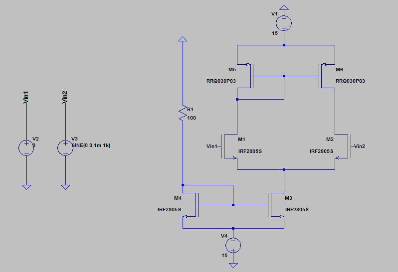
Secondly I designed this:
0j6aGh6.png


Practically when I get the drain output I have a big amplification but with a HUGE DC offset: 12 volts about!
Do you know why?Did I mistaken somehitng?

Moreover I don't remember a thing from my electronics studies: should R1 be linked to ground or to V1?

Thank you very much
 
Engineering news on Phys.org
  • #2
Perhaps it's better this way
DifferentialM.PNG

― the drain of M1 ought to be kept at the same voltage as M2.

It's better to use a dual matched pair of MOSFET in one package as M1 and M2.
 
Last edited:
  • #3
Your solution makes sense, I have some thoughts though:
First, I would like to use as less resistors as possible, like if it was an IC amplifier.
Secondly, I would like to know why my circuit offsets the voltage so much. This is basically the easiest form of differential amplifier, so there must be a problem I cannot recognize.

9s7y7ra.png


This is from the Sedra-Smith; as as you see I replaced the current source with the mirror, but the offset is still there.

What I think is that there is some problem either with transistors model, or ltspice itself. In fact I simulated an exercise from Sedra-Smith:

gC8bBlY.png


Which results are Rd=5k and Rs=3.25; and LTSpice gives different values for Id and Vd! The model I used is:

.model M1 NMOS(Vto=0.7 Kp=100u L=1u W=32u)

Is the model wrong?
 
  • #4
It may well be the channel length modulation effect (neglected in the textbook but not in LTspice) to blame. In ICs, MOSFETs with very low channel modulation must be used, otherwise all the mirrors would work wrong. With your differential amplifier, I would first try to decrease the positive supply so as to make the drain potentials (left and right) equal when both the inputs are grounded.
 
  • #5
Frank-95 said:
Practically when I get the drain output I have a big amplification but with a HUGE DC offset: 12 volts about!
Do you know why?Did I mistaken somehitng?
You are operating the amplifier in open loop. What are you measuring the huge DC offset voltage relative to.

Frank-95 said:
Moreover I don't remember a thing from my electronics studies: should R1 be linked to ground or to V1?
Ground will be quieter and heat the resistor half as much.
 
  • #6
Your output voltage, (drains of M2 and M6 ?), is centred about +12 volt above ground because that is the voltage on the drain of M5, (and on the gates of the symmetrical p-channel mirror).
 
  • Like
Likes Frank-95
  • #7
Baluncore said:
Your output voltage, (drains of M2 and M6 ?), is centred about +12 volt above ground because that is the voltage on the drain of M5, (and on the gates of the symmetrical p-channel mirror).

Oh right, my bad, that is the bias point; I've avoided that bypassing the output with a capacitor. But now an abvious questions arises: in real multistage opamp, where the output of one stage is the input of the next stage, is the dc component kept in each stage, it doesn't seem so to me, does it? Moreover, even if it does, is the output always bypassed with a capacitor in real cases?
 
  • #8
As pointed out by Baluncore we never use this type of circuit without some sort of a negative feedback to "set" DC conditions.
Frank-95 said:
Which results are Rd=5k and Rs=3.25; and LTSpice gives different values for Id and Vd! The model I used is:

.model M1 NMOS(Vto=0.7 Kp=100u L=1u W=32u)

Is the model wrong?

No, your model is just fine. I for Rd = 5k and Rs = 3.25k get Id≈400μA in LTspice
You can also use this model
.model n VDMOS (Vto=0.7 Kp=3.2m)
 
  • #9
Here is an output stage added to the differential front end.
Attached is an LTspice file diff-amp.asc. Remove the .txt extension to view or run it.
 

Attachments

  • diff-amp-1.asc.txt
    2.6 KB · Views: 445
  • BJT-diff-amp-2.asc.txt
    2.2 KB · Views: 415
Last edited:
  • #10
Jony130 said:
No, your model is just fine. I for Rd = 5k and Rs = 3.25k get Id≈400μA in LTspice
You can also use this model
.model n VDMOS (Vto=0.7 Kp=3.2m)

CbL4JyA.png


Oh I don't know, this circuit keeps on yielding 54 uA :/

Baluncore said:
Here is an output stage added to the differential front end.
Attached is an LTspice file diff-amp.asc. Remove the .txt extension to view or run it.

Thank you very much, I got your point :)
 
  • #11
Frank-95 said:
Oh I don't know, this circuit keeps on yielding 54 uA :/
Change NMOS name into M1 . Upper M1 is a transistor designation number not the sim MODEL.
 
  • Like
Likes Frank-95
  • #12
Thank you, got it!
 

FAQ: Voltage offset differential amplifier

1. What is a voltage offset differential amplifier?

A voltage offset differential amplifier is an electronic circuit that amplifies the difference between two input voltages. It is commonly used to amplify low-level signals, such as those from sensors, and reject common-mode noise. The amplifier has a high input impedance, making it suitable for measuring signals without disturbing the original circuit.

2. How does a voltage offset differential amplifier work?

A voltage offset differential amplifier works by taking the difference between two input voltages and amplifying it by a fixed gain. The amplifier has two inputs, one for the positive signal and one for the negative signal. The output is the amplified difference between the two inputs. The amplifier also has an offset voltage, which is a small voltage added to the output to compensate for any imbalances in the circuit.

3. What is the purpose of a voltage offset in a differential amplifier?

The purpose of a voltage offset in a differential amplifier is to compensate for any mismatches or imbalances in the circuit. This offset voltage is added to the output of the amplifier to ensure that the output is zero when the two inputs are equal. It helps to improve the accuracy and stability of the amplifier by reducing the effects of noise and other disturbances.

4. What are the advantages of using a voltage offset differential amplifier?

There are several advantages of using a voltage offset differential amplifier. Firstly, it has a high input impedance, making it suitable for measuring low-level signals without affecting the original circuit. Secondly, it has a high common-mode rejection ratio, which means it can reject noise and interference from the input signals. Lastly, it has a wide bandwidth, making it suitable for amplifying signals with a wide range of frequencies.

5. What are some common applications of a voltage offset differential amplifier?

A voltage offset differential amplifier has many applications in scientific research and engineering. Some common applications include signal conditioning for sensors, data acquisition systems, audio amplifiers, and precision measurement equipment. It is also used in medical devices, such as electrocardiographs and electroencephalographs, to amplify and measure biological signals.

Similar threads

Back
Top