Why does Efm shift in MOSFETs?

  • A
  • Thread starter jaus tail
  • Start date
  • Tags
    Shift
In summary, the Fermi level in an MOS structure is only constant when thermal equilibrium is reached and no external bias is applied. When the gate voltage is negative, the Fermi level in the metal shifts upwards, and when the gate voltage is positive, the Fermi level in the metal shifts downwards. This is due to the attraction of electrons from the gate and the semiconductor, respectively. The gate voltage required to maintain a flat band condition is known as the flat band voltage (VFB).
  • #1
jaus tail
615
48
Hi,
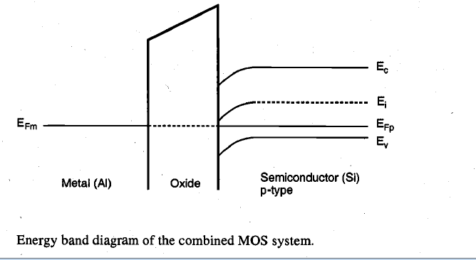
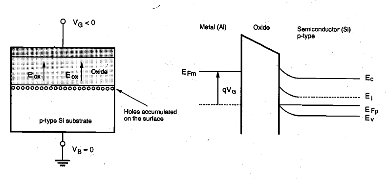
I'm studying MOSFET and the book says that when N-channel mosfet has negative or positive gate voltage, the energy band diagram will shift. I don't understand why Efm shifts.
upload_2018-9-15_14-35-31.png

Now when Vg is negative the Efm shifts upwards, Why? And when later when Vf is positive the Efm also shifts again? I don't understand this. Shouldn't Efm and Efp be at same level?
upload_2018-9-15_14-34-57.png
 

Attachments

  • upload_2018-9-15_14-34-48.png
    upload_2018-9-15_14-34-48.png
    28.3 KB · Views: 445
  • upload_2018-9-15_14-34-57.png
    upload_2018-9-15_14-34-57.png
    7.6 KB · Views: 827
  • upload_2018-9-15_14-35-11.png
    upload_2018-9-15_14-35-11.png
    34.6 KB · Views: 416
  • upload_2018-9-15_14-35-31.png
    upload_2018-9-15_14-35-31.png
    4.4 KB · Views: 1,279
Physics news on Phys.org
  • #2
The Fermi level (or electrochemical potential of the electrons) is only constant throughout a MOS device when thermal equilibrium is reached and no external bias is applied to the device..
 
  • Like
Likes jaus tail
  • #3
Thanks for the reply. Shouldn't Efm and Efp be at same level. At junction of PN diode, we shift bands after aligning the Ef of both doped regions together.
 
  • #4
  • Like
Likes jaus tail
  • #5
Thanks. This helped clear some things up. Just to be sure. Let's assume Vfb = 0 for now. initially mosfet fermi and Si fermi are at same level.
upload_2018-9-17_22-25-12.png

I got the above pic from the pdf link you gave.
Now if I apply positive Gate potential, then the positive terminal will attract electrons from Gate (metal). So the surface junction between Metal and Oxide will be devoid of electrons and so fermi level of metal will shift downwards.
Likewise the positive terminal will attract electrons from P-silicon body and fermi level of Semiconductor shifts up toward Ec at surface. Thus we bend Ec and Ev of Semiconductor so that Ec is closer to Ef at junction.

This pic helped a lot:
upload_2018-9-17_22-27-40.png

But I don't understand How Vfb helps. I assumed Vfb = 0 and was able to figure out how bands shift. But can you elaborate as to how Vfb comes in the picture?
When Vg is less than Vfb as in accumulation case, is Vg also less than zero? That would explain why negative Q accumulates at junction. Cause negative Vg repels electrons to junction.
 

Attachments

  • upload_2018-9-17_22-25-12.png
    upload_2018-9-17_22-25-12.png
    4.9 KB · Views: 627
  • upload_2018-9-17_22-27-40.png
    upload_2018-9-17_22-27-40.png
    94.6 KB · Views: 761
  • #6
From “Physics and Technology of Semiconductor Devices” by Andrew S. Grove:

The electron energies at the Fermi level in the metal and in the semiconductor of an MOS structure will, in general, be different. Such an energy difference is usually expressed as a difference in work functions, which is the energy required to remove an electron from the Fermi level in a given material to vacuum. When the metal of an MOS structure is shorted to the semiconductor, electrons will flow from the metal to the semiconductor or vice versa until a potential will be built up between the two which will counterbalance the difference in work functions. When equilibrium is reached, the Fermi level in the metal is lined up with the Fermi level in the semiconductor. Therefore, there will be an electrostatic potential variation from one region to the other, as illustrated in….

Thus, when there is a difference in work function between the metal and the semiconductor, one has band bending within the semiconductor in the equilibrium case with gate voltage VG = 0. You can now apply just enough gate voltage VG to counterbalance the work function difference and to maintain a flat band condition in the semiconductor. The gate voltage required to bring about the flat band condition is called the flat band voltage VFB. VFB is - so to speak - the reference point for the gate voltage VG for further considerations.
 
Last edited:
  • Like
Likes jaus tail

Related to Why does Efm shift in MOSFETs?

1. Why does Efm shift in Mosfets?

Efm (Fermi energy level) shift in Mosfets (metal-oxide-semiconductor field-effect transistors) is caused by the presence of an electric field at the interface between the metal gate and the semiconductor channel. This electric field attracts or repels electrons at the interface, leading to a change in the energy level of the electrons, known as the Efm shift.

2. How does the Efm shift affect the performance of Mosfets?

The Efm shift can significantly impact the performance of Mosfets as it affects the threshold voltage, which is the minimum voltage required to turn on the transistor. A larger Efm shift can result in a change in the threshold voltage, which can affect the switching behavior and overall efficiency of the Mosfet.

3. What factors can cause Efm shift in Mosfets?

Efm shift in Mosfets can be caused by various factors such as the gate material, the thickness of the oxide layer, the doping concentration of the semiconductor channel, and the temperature. These factors can affect the electric field at the interface and, therefore, contribute to the Efm shift.

4. Can the Efm shift be controlled or minimized in Mosfets?

Yes, the Efm shift can be controlled or minimized by carefully selecting the materials and parameters of the Mosfet. For example, using high-k dielectric materials for the gate can reduce the electric field at the interface, resulting in a smaller Efm shift. Additionally, precise fabrication techniques can also help minimize the Efm shift.

5. Are there any applications where Efm shift in Mosfets is desirable?

Yes, there are applications where Efm shift in Mosfets is desirable. For instance, in non-volatile memory devices such as Flash memory, the Efm shift is used to trap and store charges in the oxide layer, allowing for data storage. Similarly, in floating-gate Mosfets used in analog circuits, the Efm shift is utilized to store charge and alter the threshold voltage, enabling analog signal processing.

Similar threads

  • Atomic and Condensed Matter
Replies
4
Views
2K
  • Atomic and Condensed Matter
Replies
1
Views
1K
  • Introductory Physics Homework Help
Replies
9
Views
941
  • Electrical Engineering
Replies
13
Views
297
  • Atomic and Condensed Matter
Replies
1
Views
2K
  • Electrical Engineering
Replies
4
Views
4K
Replies
3
Views
3K
  • Engineering and Comp Sci Homework Help
Replies
5
Views
3K
  • Atomic and Condensed Matter
Replies
2
Views
3K
  • Introductory Physics Homework Help
Replies
1
Views
512
Back
Top