Why Does the Common Base Amplifier Model Show a Steep Rise and Offset?

In summary: Neither of these articles mention the steep rise and offset you are seeing. Changing DC bias will change the base-emitter resistance, but it is not due to over-simplification as he claims on the first site. He might be referring to the saturation region of the transistor. The advantages and disadvantages of using a FET or an inverting opamp in a low input impedance amplifier are mostly frequency dependent. Both options have their own advantages and disadvantages.
  • #1
haminous
7
0
Greetings. I am trying to understand the common base amplifier better so I can build a preamp for a low impedance guitar pickup. In order to explore its operation, I tried to model it with the "approximated" Ebers-Moll model (from the wikipedia page on BJT's) and the graphing program in Mac OSX.
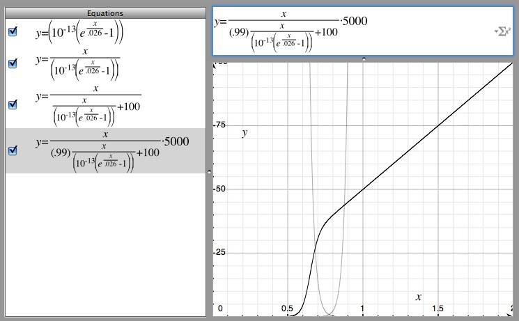
Graph.jpg


The first equation is the emitter current (Y) relationship to base-emitter voltage (X). The second puts (X) over that equation to give the resistance. The third adds 100 ohms (as the input resistor) and puts (X) over the that again to give the new base current. The fourth and highlighted equation is supposed to be the collector current (with the addition of the 0.99 coefficient for alpha) times the output resistor to give the input to output voltage relationship. This was supposed to be a very generic and ideal model (hence the lack of base-emitter resistance or accounting for saturation) just for me to visualize what is going on and play with the numbers. But, as you can see, the graph does not look like what it should. There is a steep rise over about 0.6 to 0.8 volts and then a slope that looks like is has about the right gain, just shifted up way too high. Where does that steep rise and offset come from as opposed to a regular transistor model? Is it due to over-simplification? I would really like to understand the mathematical relationships here.

I am also extremely curious why, according to the author of this site: http://www.allaboutcircuits.com/vol_3/chpt_4/7.html" , changing the DC bias changes the base-emitter resistance, thus affecting the gain.

And, finally, if anyone can provide some insight... What would be the advantages and disadvantages of using either a FET in the common gate arrangement or an inverting opamp with a low input impedance?

Thanks in advance for your time.
 
Last edited by a moderator:
Engineering news on Phys.org
  • #2
Can't help you with the modelling, but any transistor's base emitter junction behaves just like a diode. It does not conduct in the forward direction until it has a minimum voltage on it.

This voltage is typically 0.6 volts. So, unless the transistor gets this voltage, it will not get any base current, so the collector current will also be zero.

This is usually supplied in the form of base bias with suitable resistors and the bias current is modified by incoming signals to get amplified in the transistor circuit.

You could use a FET in common gate mode, but I don't think it is done at all. You would lose the high input impedance and also the fairly good isolation between output and input that a FET has in common source mode.

Low input impedance is not usually an advantage or desirable. Whatever drives a low impedance has to be low impedance itself and in most practical circuits, this is not the case.
Especially driving from a tuned circuit becomes very difficult as the damping of a low input impedance increases the bandwidth of the tuned circuit and limits the voltage you can get out of the tuned circuit.

Try modelling a common emitter amplifier. They are much more useful than common base ones and they will help you understand common base more easily.
 
  • #3
Thanks for your suggestions, vk6kro. I am indeed interfacing with a low impedance source, probably in the range of tens to hundreds of ohms with not much power, so I am trying to design a preamp utilizing the maximum power transfer theorem. Interestingly, you noted that a low impedance input will widen the bandwidth of a tuned source; while a guitar pickup is not a tuned circuit per-se, it is reactive and I would like to get the highest bandwidth possible.
 
  • #4
You do not need to use the maximum power principle to drive a voltage amplifier.
Doing that loses you half your signal voltage.

Amplifiers that have a high input impedance can be driven adequately with low impedance sources. In this case, the high impedance amplifier gets most of the signal voltage from the source.

As you may have found, the input impedance of common base amplifiers can be just a few ohms even though you might be putting your input signal across a few hundred ohm resistor.
This is almost never an advantage which is why common base amplifiers are hardly ever used.
 
  • #5
Also, common base amps are prone to oscillation because there is no phase shift between input and output.
 
  • #6
Hmmm..OK. Thanks for the input. So, just out of curiosity, what about a cascode configuration? Would be the advantages and disadvantages?
 
  • #7
Probably a cascode FET amp would be worth trying.
Depends. How much gain do you need and do you have to tailor the frequency response?

If you have to tailor the response, you should probably look at dedicated preamp chips.

Wikipedia has a good article on Cascode Amplifiers.
http://en.wikipedia.org/wiki/Cascode

I found this article that just uses a single FET for a guitar amp.
http://www.till.com/articles/GuitarPreamp/
His comments about impedance make interesting reading.
His amp would have a voltage gain of about 3, but a much lower output impedance than input impedance which is good.
 
  • #8
Interesting. It might be fun to try to implement with tubes just for kicks someday. I need a healthy amount of gain, but a just a flat, wide response.

I think I may have found my error with the graph, but I haven't sat down to work out the math yet.

Thanks for all the advice
 
  • #9
I am a second year electrical engineering student. I m investigating the design of common emitter, common emitter with fixed gain, common collector, common base, common collector to base feddback with curreent mirror. I would like t ask what is the use of each component in the design and how the input signal get amplified. what the bypass capacitors do. this will inprove m knowledge on amplifiers

kinds regards

chite


vk6kro said:
Can't help you with the modelling, but any transistor's base emitter junction behaves just like a diode. It does not conduct in the forward direction until it has a minimum voltage on it.

This voltage is typically 0.6 volts. So, unless the transistor gets this voltage, it will not get any base current, so the collector current will also be zero.

This is usually supplied in the form of base bias with suitable resistors and the bias current is modified by incoming signals to get amplified in the transistor circuit.

You could use a FET in common gate mode, but I don't think it is done at all. You would lose the high input impedance and also the fairly good isolation between output and input that a FET has in common source mode.

Low input impedance is not usually an advantage or desirable. Whatever drives a low impedance has to be low impedance itself and in most practical circuits, this is not the case.
Especially driving from a tuned circuit becomes very difficult as the damping of a low input impedance increases the bandwidth of the tuned circuit and limits the voltage you can get out of the tuned circuit.

Try modelling a common emitter amplifier. They are much more useful than common base ones and they will help you understand common base more easily.
 
  • #10
The common-base npn amplifier is basically a dc-coupled impedance transformer. See the plot of the two sine waves in
http://www.allaboutcircuits.com/vol_3/chpt_4/7.html
The same current (within a few percent) is flowing in the 100-ohm input impedance resistance and in the 5000 ohm output impedance. The voltage gain is ~50. If you are familiar with grounded grid amplifiers, the concept is the same.

Bob S
 

FAQ: Why Does the Common Base Amplifier Model Show a Steep Rise and Offset?

What is a common base amplifier?

A common base amplifier is a type of electronic circuit that amplifies a weak signal and produces a larger output signal. It is commonly used in audio and radio frequency applications.

How does a common base amplifier work?

A common base amplifier consists of three components: a transistor, a resistor, and a power supply. The transistor acts as a switch, controlling the flow of current through the resistor. As the input signal is applied to the base of the transistor, it modulates the current and produces a larger output signal.

What are the advantages of using a common base amplifier?

Common base amplifiers have a low input impedance, making them ideal for applications where the input signal has a low impedance. They also have a high voltage gain, making them suitable for amplifying weak signals. Additionally, common base amplifiers have a wide frequency response, making them useful in a variety of electronic devices.

What are the limitations of a common base amplifier?

One limitation of a common base amplifier is that it has a low input resistance, which can cause a significant amount of power to be dissipated in the input resistor. This can lead to thermal instability and reduced overall performance. Additionally, common base amplifiers have a high output impedance, which can affect the stability and accuracy of the output signal.

How can common base amplifiers be modeled?

Common base amplifiers can be modeled using various techniques, such as the hybrid-π model or the T-model. These models use simplified circuits to represent the behavior of the amplifier and can be used to analyze and design common base amplifiers for specific applications.

Similar threads

Replies
17
Views
3K
Replies
1
Views
3K
Replies
5
Views
2K
Replies
13
Views
5K
Replies
2
Views
9K
Replies
1
Views
1K
Back
Top