Why is the opamp output a voltage?

In summary, an OP amp with a voltage output will have a high input impedance and a low output impedance.
  • #1
jaydnul
558
15
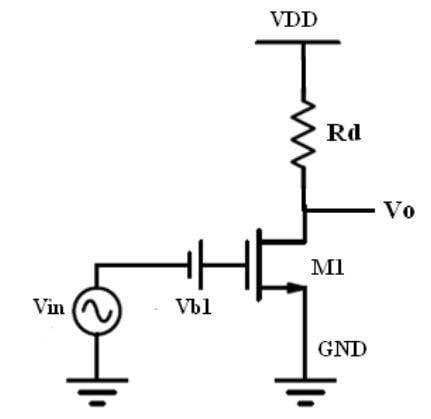
Take the following circuit:
noiseamp5.jpg


The transistor turns the voltage input into a proportional current. Then it is said the resistor Rd turns the current back into a voltage. Then to calculate the output impedance of this circuit you would take Rd in parallel with the transisor's r0.

But If you add a load resistor to the voltage output, then you will be adding it in parallel with the output resistance, not in series. This doesn't make sense if it is a voltage source output. Hopefully you can see my confusion.

Thanks
 
Engineering news on Phys.org
  • #2
jaydnul said:
Then it is said the resistor Rd turns the current back into a voltage.
Right, via Ohm's Law. This assumes an open circuit voltage.
jaydnul said:
But If you add a load resistor to the voltage output, then you will be adding it in parallel with the output resistance, not in series.
If the load has a low resistance, then yes, you will load down the output stage and will have diminishing amplification. Ideally the load resistance will be large compared with the output resistance of the circuit you have above, so the load resistance can be ignored.
 
  • Like
Likes jim hardy
  • #3
jaydnul said:
Why is op amp output a voltage?
Within the operation limits it is because of the feedback circuit which (according to the voltage type input) will adjust the output voltage.
 
  • #4
Plot V versus I for any real world device. If part of the curve is nearly horizontal we call it constant voltage. If it is nearly vertical, we call it constant current. But in real life, these curves are seldom exactly horizontal or vertical over a wide range. So yours is a question of language, not physics.

Here is an example except it plots I versus V instread of V versus I. It is for a solar panel. We could call it a current source or a voltage source in different ranges.

1450315156.gif
 
  • #5
jaydnul said:
Take the following circuit:
What opamp has that for its output stage? If there is one, it must be pretty limited in its applications...
 
  • #6
jaydnul said:
This doesn't make sense if it is a voltage source output.
The Collector of the transistor is not a 'voltage source'. (That may solve your misunderstanding) The circuit shown is a Common Emitter Configuration. The current into the collector will be determined by the current into the Base (as long as the Vce is in the right range for the transistor to be operated. If you connect a resistor from the Collector to Ground, the current through RD will be the sum of currents through transistor and load resistor and the Collector/Ground volts will be lower.
 
  • Like
Likes jim hardy
  • #7
jaydnul said:
you would take Rd in parallel with the transisor's r0.
But what value would you assign to the collector r0? It varies so as to keep the Collector current to the value the Base is telling it. That involves a Variable Resistor so best to steer clear of that!
If you were to consider an AC amplifier - with a Capacitor in series with the Rd, it may be easier to think in terms of the collector load and the output load in Parallel. Lower AC gain but the same DC Collector volts. OR, you could connect the Load resistor to the + supply and the two resistors really would be in parallel, pulling Vc up and not down.
Bottom line here is that the 'Gain' of the circuit can be defined in various ways: Iout/Iin, Vout/Vin, Iout/Vin, Vout/Iin, depending on the way it's connected. The term Transistor came, I believe, from Transfer Resistor which would be a V over an I. But modern transistors have tiny Ib and high current gain so, with a few externally connected resistors, they make very handy Voltage Amplifiers - just like triode valves. And AC amplifiers are a lot easier than DC amplifiers because the DC conditions can be sorted out separately from the AC signal path.
 
  • #8
Op amp output can be a current source. Do a search on "operational transconductance amplifier". This type of amp has a high impedance current output.

Claude
 
  • Like
Likes berkeman
  • #9
We need to clear things up. There seem to be conflicting arguments going on but neither is actually wrong. it's just Context. The only explicit circuit in the thread is a single transistor with a collector that acts as a current source (in the OP). That's what I was commenting on. As part of an integrated OP amp, that output transistor will have feedback to keep the voltage constant, independent of the load (usual warnings about operating conditions apply) i.e. a voltage source.
Look at the whole schematic diagram of any OP amp and its minimum configuration gives it a high input impedance and a low output impedance. That is a very different matter though. You can do ANYTHING with the appropriate feedback and people mostly like to use Voltage Amplifiers in their designs, except when there is something special required due to the circuit they are placed in.
 
  • Like
Likes jim hardy
  • #10
But the output feedback network may differ for an OTA. With traditional op amp, feedback consists usually of 2 branches, output to inverting input, & inverting input to ground. In an OTA, the feedback network is ofter just an R-C network to ground, or it can be like the one just described.
The OTA, outputs a high Z current source from a bjt collector. This current is then fed into an R-C feedback network & translated into a voltage. With traditional op amp, a divider network is placed on the output. The op amp output is low Z voltage source. The divider provides a divided down voltage at the inverting input.
Later today, if I can find it, I'll post a TI app note which details the OTA.

Claude
 
Last edited:
  • #11
jaydnul said:
But If you add a load resistor to the voltage output, then you will be adding it in parallel with the output resistance, not in series. This doesn't make sense if it is a voltage source output. Hopefully you can see my confusion.
Thanks

Short answer: The transistors output current develops a voltage across RD - however, this does not mean that the output node would be a voltage source.
By defibition a voltage source has a very small (ideally zero) source resistance. If you connect any load to a non-ideal source (like the drain node) the voltage goes down, of course!.
 
  • #12
LvW said:
Short answer: The transistors output current develops a voltage across RD - however, this does not mean that the output node would be a voltage source.
However, a typical opamp (within its environment and within its operation limits) would (with quite good accuracy). Regardless of the exact type of its output stage (what, without much reason were made to the center of the question discussed).
 
  • #13
Rive said:
Within the operation limits it is because of the feedback circuit which (according to the voltage type input) will adjust the output voltage.
I don`t think that it is the feedback circuit which is responsible for the fact that the classical opamp can be regarded as a voltage source.
Counter example: Transistor stage with negative feedback.
Instead, the "naked" opamp is designed with a rather small ouput resistance and, thus, can be regarded as a voltage source.
The main purpose of the feedback circuit is to adjust/fix the desired GAIN value.
(As a nice side effect, the output resitance is further reduced).
 
  • #14
But that GAIN is actually output VOLTAGE per input VOLTAGE right?

... So at the end (by the definition of GAIN) you will get output VOLTAGE because there is a feedback circuit which will grant you that?
 
  • #15
Rive said:
But that GAIN is actually output VOLTAGE per input VOLTAGE right?

... So at the end (by the definition of GAIN) you will get output VOLTAGE because there is a feedback circuit which will grant you that?

An offset-compensated opamp with an open-loop gain of 1E5 (and without feedback) produces an output voltage of 1V if the input signal is 10µV.
As mentioned, it is the purpose of the feedback circuit to reduce this unwanted excess gain to a suitable value.
 
  • #16
That's not 'unwanted excess gain', but the primary minimal requirement to have an OpAmp for practical use.

The open loop gain is so high exactly because who dreamed up this device class wanted to use it with feedback to get a linear characteristics (side effect is that the output would work as a voltage source within operation limits, regardless of the exact type of the output stage).
 
  • #17
Yes - I agree that the term "unwanted excess gain" is misleading.
What I mean (as you certainly know) is that we do not use practically this high open-loop gain directly for linear amplifying purposes (without negativ feedback) .
Thanks for correcting my wording.
 
  • Like
Likes sophiecentaur
  • #18
The OP question stated OP AMP. But, the diagram shows a single stage FET amp.
Regarding the current/voltage source question, LvW, the output of a collector or drain is indeed a high Z current source. Such i s the case with an OTA. But a traditional OP AMP has an emitter or source folloiwer output stage. The output of an emitter follower is low Z. As load imp stance varies, emitter follower output voltage hardly changed. An e.g. stage is a buffer, high Z in, low Z out. Thus it behaves like voltage source.

Claude
 
  • Like
Likes jim hardy
  • #19
jaydnul said:
But If you add a load resistor to the voltage output, then you will be adding it in parallel with the output resistance, not in series.

Of course you are placing it in parallel. That effectively lowers R0.

Then you calculate voltage gain using that parallel combination of Ro and Rload.

No problem. Work some exercise problems.
 
Last edited:
  • #20
cabraham said:
... LvW, the output of a collector or drain is indeed a high Z current source.

Claude - I rather think, we do not have a clear wording for the "source characteristics" available at the drain node of the shown circuit.
High Z current source? What means "high"? A source resistance of 5 or 10 kohms (instead of infinite)?
And why not a non-ideal voltage source with a finite source resistance (instead of zero)?

To me, we only can say that an electrical source can be (nearly) seen as a
* voltage source as long as a connected load resistance will alter the value of the resulting voltage by an acceptable small amount only,
(current is primarily determined by the load)
* current source as long as a variation of a connected load resistance will alter the value of the resulting current out of the source by an acceptable small amount only,
(voltage is primarily detrermined by the connected load).
 
  • #21
cabraham said:
The OP question stated OP AMP. But, the diagram shows a single stage FET amp.
Similar (current) boost extension are often used for OpAmps in some circumstances. It can be considered as an external output stage. It has just very limited significance in regards of the original question.
 
Last edited:
  • #22
LvW said:
Claude - I rather think, we do not have a clear wording for the "source characteristics" available at the drain node of the shown circuit.
High Z current source? What means "high"? A source resistance of 5 or 10 kohms (instead of infinite)?
And why not a non-ideal voltage source with a finite source resistance (instead of zero)?

To me, we only can say that an electrical source can be (nearly) seen as a
* voltage source as long as a connected load resistance will alter the value of the resulting voltage by an acceptable small amount only,
(current is primarily determined by the load)
* current source as long as a variation of a connected load resistance will alter the value of the resulting current out of the source by an acceptable small amount only,
(voltage is primarily detrermined by the connected load).
AS far as voltage being determined by the connected load, that would be the case for the common source GET amp in the OP schematic, as well as an OTA type of amp. The OP question reads "why is OP AMP output a *voltage*, but then illustrates a CS FET stage where output is current, voltage being determined by load Z.
I agree with what you said for the illustrated schematic on OP. But in a traditional low Z output op amp, is not the final stage which drives the load an emitter follower or source follower? What are the properties? It has low Z output. The impedance at the emitter terminal of an effort is simply input impedance presented to the base, divided by (hfe+1). Generally Z out is a low value around 30 to 50 ohms. Say the signal generator driving the input is 50 ohms. The output Z at the emitter is 50/(hfe+1). For an hfe value of 124, typical. Zout = 50/(124+1) = 0.40 ohm. As long as the output load impedance is much larger than this 0.40 ohm value, the load impedance has negligible influence on output voltage. The current varles inversely with Zload.
Did I help?

Claude
 
Last edited:
  • #23
Also remember please, that op amps use feedback to maintain constant voltage output. It is desirable that output Z be as low as possible, preferably below 100 ohms. If we used common source or common emitter stage at the output of the op amp, the output Z is tens to hundreds of kohm. The output Z with the feedback loop closed is the open loop value divided by loop gain. So if Zout open loop is 200 kohm, with 60 dB loop gain, or 1000 factor, the Zout cloised loop is aroung 200k/1000 or 200 ohms, not great, but acceptable in some applications.
In rf designs, such as filtering, if the highest frequencies approach the gain bandwidth limit of the op amp, loop gain is a low value. So at a high enough frequency, instead of 60 dB loop gain, there could be 40 dB, or even 20 dB. Zout would be 2000 ohm, or 20 kohm.
A good reference book on op amps covers the subject in detail. I recommend books by Jerald Graeme.

Claude
 
Last edited:
  • #24
Rive said:
But that GAIN is actually output VOLTAGE per input VOLTAGE right?

... So at the end (by the definition of GAIN) you will get output VOLTAGE because there is a feedback circuit which will grant you that?
Not really. That is a very limited definition of 'Gain' and it may appear to confirm your view. But your 'Gain' is in fact 'Voltage Gain' (which is how you have defined it).
The default definition for the naked word Gain is actually 'Power Gain'. That takes account of possible differences in input and output circuit Impedances.
 
  • #25
As you will know, Rb is in fact in parallel with the load in which respect to the output AC signal. The equivalent circuit of the output of the transistor is not more than a convenient idealization that can modelate the device in small signal. Different models exists, made all out of ideal current sources, ideal voltage sources, resistors, capacitors, etc. The real device is not a current or voltage source. Do a search for Thevenin equivalent circuit and Norton equivalent circuit. It seems that Sophiecentaur did not noticed that your transistor is a FET and not a BJT.
 
  • #26
Fernando Perfumo said:
It seems that Sophiecentaur did not noticed that your transistor is a FET and not a BJT.
You got me there. But the important thing was that what was shown was not an OP Amp and the device output impedance is high. The only way to produce a 'voltage source' with what is shown would be to have a very low Rd which would make the Voltage Gain and efficiency extremely Low.
 
  • #27
sophiecentaur said:
You got me there. But the important thing was that what was shown was not an OP Amp and the device output impedance is high. The only way to produce a 'voltage source' with what is shown would be to have a very low Rd which would make the Voltage Gain and efficiency extremely Low.
Of course, it is not an Operational amplifier. :)). Jadnull is I am convinced, a clever person, just he need to digest fully this things.
 
  • #28
sophiecentaur said:
Not really. That is a very limited definition of 'Gain' and it may appear to confirm your view. But your 'Gain' is in fact 'Voltage Gain' (which is how you have defined it).
One would expect some enlightening power from the included >>that<< word there.

Yes, really: that gain what the topic is actually about is voltage gain.
Quite hard to find anything else regarding OpAmps. A type of 'current gain' is a special topic, but still exists: but to provide a power gain based on OpAmps would require a quite complex feedback circuit, possibly with a multiplier. Closest to this would be some measurement circuits I think, but those usually has no 'power' output.

Title of topic:
Why is the opamp output a voltage?
After that, the content of topic chewing on the fact that an output stage alone will always act as an output stage (alone).
 
  • #29
Rive said:
Yes, really: that gain what the topic is actually about is voltage gain.
As the thread had included other transfer characteristics then the context was not as clear as you imply and the passage I challenged seemed to be excluding this.
I looked at this link for some support and they make it clear that the Gain can refer to the relationship between all combinations of input and output signals. Page 7 sets the context for OP Amp discussions. Signal Power often tends to be ignored or tacitly implied in the context of OpAmps.
However, even Voltage Gain value is not sufficient in many contexts. The Power gain for an amplifier with different input and output impedances is not equal to the Voltage gain. Perhaps it's my RF experience that makes me all too aware of this. A mains transformer with a ratio of 1:10 may produce an 'Voltage Amplification factor of 10 but it is in no way an 'Amplifier' of the Input Power. It always annoys me when the bones of the middle ear are said to "amplify" the sound received when they are, in fact, matching devices.
 
  • #30
Hopeless academic overthinking on a clearly defined topic what's completely missing the very point at the end.

The OP stated a narrow focus question, and it was widened to a such useless scope that at the end it cannot be answered clearly - and it is still progressing further.
 
  • Like
Likes cabraham
  • #31
Rive said:
Hopeless academic overthinking on a clearly defined topic what's completely missing the very point at the end.

The OP stated a narrow focus question, and it was widened to a such useless scope that at the end it cannot be answered clearly - and it is still progressing further.
Yes, you have a point but it is also important to keep things clear and to avoid generalisations. You must be aware of the problems about using dB Gain figures that come about when people aren't aware of the pitfalls.
"Are those Voltage dBs or Power dBs?" is so often asked and that's why I am being picky. That's not "academic overthinking", it's avoiding elementary mistakes.
 
  • Like
Likes jim hardy
  • #32
Rive said:
Hopeless academic overthinking on a clearly defined topic what's completely missing the very point at the end.
The OP stated a narrow focus question, and it was widened to a such useless scope that at the end it cannot be answered clearly - and it is still progressing further.
I agree with you.
Besides the fact that the OP has selected a wrong title, everythig he has stated was correct.
However, he did not explain the source of his his confusion. May be that`s the reason for the various answers.
 
  • #33
LvW said:
Besides the fact that the OP has selected a wrong title
I think he choose the correct title, with a terrible example. For OpAmps the output stage defines only the operation limits/area: within those limits the output can be determined through the feedback. Any usage when the output (or something else) is a limiting factor instead of the feedback can be considered as faulty.
Since he did not know this, he thought that the answer will be related to the output circuitry. The answers followed this path and the topic started to diverge from the title and kept on giving more and more generalised answers, based on the commonly used output stages (and non-opamp related definitions).

That's how I see it.
 
  • Like
Likes sophiecentaur
  • #34
This is the most typical op-amp, according to Wikipedia:
750px-OpAmpTransistorLevel_Colored_Labeled.svg.png

We see the input voltage difference converted into proportional current that is charging the 30 pF capacitor. The capacitor voltage is added to the (Q15 base potential which is almost the) "Vs-" potential and the result is applied to the input of the output voltage follower thus defining the output potential.
 
Last edited:
  • Like
Likes berkeman
  • #35
AlexCaledin said:
charging the 30 pF capacitor.
It's not really "charging" that capacitor. That is likely the "dominant pole" setting capacitor for the opamp, which is needed for stability when the opamp is used in feedback configurations.

http://m.eet.com/media/1126333/266795-6666155_fig2.gif
266795-6666155_fig2.gif
 
  • Like
Likes AlexCaledin
Back
Top