Controlling an electronic load across two ground domains

In summary: Yes, you would make a miller integrator by connecting the (-) input of U3 to the junction of R2 and C1.
  • #36
Sorry @Tom.G, I rationalised and completely turned the circuit around. I think you missed the point that the AD629 isolation amplifier is now being used to sense the DAC voltage and zero reference across the isolation barrier. Power derived from the load supply is then used to run everything needed to regulate the load current.
The DAC (that was once a pot) is not connected directly to the floating load ground, it is powered and driven by the processor or whatever controls it, only it's output voltage is exposed as a floating voltage source to the inputs of the AD629.

The 50V, 50Hz AC supply is there to demonstrate, or test, the common mode rejection of the floating grounds when using the AD629.

For my simulation I define the LTspice simulation ground for the floating load circuit because simulation becomes very slow when there are high resistance ties across the simulation matrix.

Here is a revised schematic with very minor changes. Still no symbol for the AD629.
floatgnd2.png
 
Engineering news on Phys.org
  • #37
Baluncore said:
Still no symbol for the AD629.
Enter AD629 in the "Product" field at this website:
https://www.analog.com/en/design-center/simulation-models/spice-models.html
It will probably work in most cases. If the AD629 fails to function as an op-amp, as when its supply voltage disappears, things could get 'interesting.'

Sounds like a Smoke Test will resolve the question.

Cheers,
Tom
 
  • #38
Tom.G said:
It will probably work in most cases. If the AD629 fails to function as an op-amp, as when its supply voltage disappears, things could get 'interesting.'
If the power supplies disappear there will be no current to control. The AD629 would then have 680k resistors from an externally powered DAC to the chip static protection diodes, with 3 uA flowing per volt of supply offset. How could that be interesting?

Tom.G said:
Sounds like a Smoke Test will resolve the question.
What question? Your Fear, Uncertainty and Doubt over what? How could my circuit be any worse than using the AD629 to sense the current across the ground discontinuity?

I have the AD629 models from ADI wrapped in a demonstration LTspice symbol from the LTspice group, that is not directly applicable to a schematic like mine. I can make one if I really need it, but the symbol used by gnurf looks OK.
@gnurf
1. Can you please post your AD629.sym and hopefully AD629.sub model files for LTspice, extend with .txt to attach, or PM for an email address.
Re: diagram in post #27.
2. To test the isolation between grounds; replace R20 = 1 MEG with an AC sinewave voltage source of 50 Hz, 50 volts. See if that shows up in the output.
3. What is the purpose of R14?
 
  • #39
Baluncore said:
@gnurf
1. Can you please post your AD629.sym and hopefully AD629.sub model files for LTspice, extend with .txt to attach, or PM for an email address.
Re: diagram in post #27.
2. To test the isolation between grounds; replace R20 = 1 MEG with an AC sinewave voltage source of 50 Hz, 50 volts. See if that shows up in the output.
3. What is the purpose of R14?
  1. See attachments.
  2. Plot with a SINE(0 50 50) source in parallel to R20:
    PF_test.png
  3. It's just a residue from earlier experimenting with different (larger) sense resistors. See datasheet p. 12 for more info. It can be ignored here.

(I'll get back to earlier posts as soon as possible.)
 

Attachments

  • AD629.asy.txt
    823 bytes · Views: 183
  • AD629.cir.txt
    2.8 KB · Views: 181
  • #40
@gnurf
How goes the design ?
In my circuit a precision op-amp with negative supply rail input voltage capability will be needed for the currents sense. Any preferences?
Attached is latest version.
 

Attachments

  • float_gnd.asc.txt
    6 KB · Views: 271
  • float_gnd.plt.txt
    374 bytes · Views: 183
  • #41
Baluncore said:
@gnurf
How goes the design ?
In my circuit a precision op-amp with negative supply rail input voltage capability will be needed for the currents sense. Any preferences?
Attached is latest version.
Back at it now. I'm following your lead here and I'm re-doing the whole thing. I've causally picked AD8565 in my simulation and it seems to behave OK. Not that it worried me much, but the ground noise seen in post #39 is more or less gone in your circuit. I haven't tried to analyse why that is yet and I hope to come back to some of the other details as well at a later point. Right now I need to get this out of the door asap.

Your help has been invaluable, thank you.
 
  • #42
OK, then I will put a bit more thought into the sticking points of my current design.

Attached is latest trial circuit. OP-amp choice is not yet fixed. Look for oscillation due to the step from DAC input.

The AD8565 selection has a few problems. Vos = 10mV max, and low 16V supply voltage = fragile.

Because the integrator is also the error amplifier there was a problem with all changes to the +input appearing immediately on the source of the mosfet. To reduce that change below the slew rate of the integrating diff-amp I have a simple RC LPF on the diff-amp +input.

The DAC has 1mV steps so we might need feedback from current sense to have similar accuracy. That means less than 1 mV offset voltage or the current might not turn off.

Precision op-amps are accurate, but do not tend to include the supply rails in the common mode range. For that reason the current sense amp needs to get away from the ground rail before it provides the approx 40* gain. We must either move the sense resistor in the circuit, or shift the sense voltage before amplification to a reasonable signal level.

Shifting Vsense to Vcom at 5V means a x1 diff-amp would have input voltages of 2.5V, which seems to be a good solution. Maybe we can get some gain there also. A gain of 2 would have input voltage 1.66V, but choice of gain is limited when identical 1% or 0.1% precision resistors should be used from the same batch.

Then we pick a precision op- amp with Vos = 250uV or less. There is then no rail to rail performance required of the input or output. The common OP07, x7 series can be considered.

Changing the subject to the supplies.
The pre-regulator needs protection from the 60V supply so a cheapest 120V or higher N-chan mosfet follower (as used earlier) is simple. The problem with that circuit was that it needed a load to stabilise it, op-amps do not use enough current, hence the resistive load where Vcom is generated.

Vcom does not have to be accurate but it must be quiet. It also needs to both source and sink current, I expect about 10mA. Maybe an op-amp voltage follower to buffer a 5v reference would be a solution.

How fast will he DAC input change, ie what bandwidth is required ?
What are the implications of current error, or offset DAC code zero current ?
Consider what the cost might be of making a mistake in modelling or prototyping.
How many will be built in first batch ?
How many of these will be built before a new PCB circuit might be considered ?
 

Attachments

  • float_gnd 6.asc.txt
    6.6 KB · Views: 197
  • float_gnd 6.plt.txt
    359 bytes · Views: 182
  • #43
Baluncore said:
The AD8565 selection has a few problems. Vos = 10mV max, and low 16V supply voltage = fragile.
Based on the model and result below, is it safe to assume that about 2mV of voltage offset is included in the AD8565 model? To see what the effect of the worst case 10mV looked like in the actual circuit, I added a 10mV voltage source in series with each negative AD8565 input (I guess that makes it about 12mV total, but whatever) and the result was about 0.1A increase in the load current compared to the case without the added 10mV source. As a result, the load current for a 0V DAC control signal was 0.1A.

PF_Vos_test.png


Is that a valid way to evaluate your concern about the Vos=10mV(max)?

Baluncore said:
Changing the subject to the supplies.
The pre-regulator needs protection from the 60V supply so a cheapest 120V or higher N-chan mosfet follower (as used earlier) is simple. The problem with that circuit was that it needed a load to stabilise it, op-amps do not use enough current, hence the resistive load where Vcom is generated.
Why do you prefer to roll your own like that, and not use a monolithic regulator such as e.g., ZXTR2012P5? I haven't checked the thermal specs but if need be they're so small you could even let each opamp have their own...?

https://www.diodes.com/assets/Datasheets/ZXTR2012P5.pdf
Baluncore said:
Vcom does not have to be accurate but it must be quiet. It also needs to both source and sink current, I expect about 10mA. Maybe an op-amp voltage follower to buffer a 5v reference would be a solution.
At last our two great minds thought alike--I already thought about this...!
Baluncore said:
How fast will he DAC input change, ie what bandwidth is required ?
What are the implications of current error, or offset DAC code zero current ?
Consider what the cost might be of making a mistake in modelling or prototyping.
How many will be built in first batch ?
How many of these will be built before a new PCB circuit might be considered ?
Bandwidth is not big concern. As for the current error, as long as it's within reason it should be OK as there's an outer loop where the total load current (sensed high side to include the now increased quiescent current) is fed back to the MCU across another AD629. Zero code current is a bit more worrying though. I can probably live with whatever the opamps draw from the DUT supply, but the FET needs to turn completely off imo.

I'll come back (famous last words) to the other interesting points that have been brought up later. Thanks!
 
  • #44
gnurf said:
Is that a valid way to evaluate your concern about the Vos=10mV(max)?
No. That is plotting the open-loop gain. You must calculate the worst case Vos implications.

Code 4095 represents 4.096? volts which results in 1.024 amp. One LSB code is 0.25 mA.

The voltage across the 0.1 ohm sense resistor is obviously 0.1 volt per amp. One LSB code will give 0.1 / 4096 volt = 25uV. So each offset of 25uV will offset the zero current by one code.

Multiplying the signal by 40 relieves the problem. One code is then 1mV at the error amp.

gnurf said:
Why do you prefer to roll your own like that, and not use a monolithic regulator such as e.g., ZXTR2012P5?
No problem. I do not have a model for that, and I think it needs to be closer to 13V to handle the common mode input range of the op-amps, OP27 and OP37 which are needed to meet the 25uV per LSB without a zero offset trim adjustment. If needed, such an adjustment would eliminate the zero errors of the DAC, AD629 and op-amps.

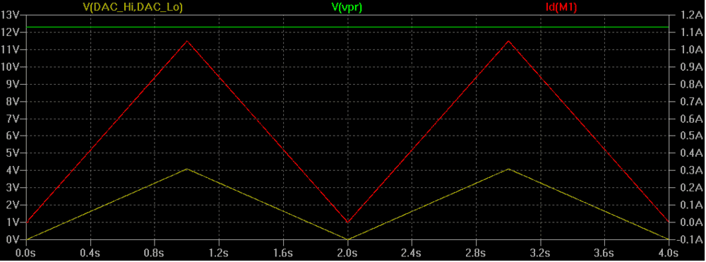
Attached is my latest version that uses the OP27 to level shift the sense voltage, then OP37 for the 40x gain, followed by OP27 for the error-amp integrator. Note slew rate now referenced to Vcom, and Vpr = 13 volt.
 

Attachments

  • float_gnd 7.asc.txt
    6.6 KB · Views: 174
  • #45
gnurf said:
To see what the effect of the worst case 10mV looked like in the actual circuit, I added a 10mV voltage source in series with each negative AD8565 input (I guess that makes it about 12mV total, but whatever) and the result was about 0.1A increase in the load current compared to the case without the added 10mV source. As a result, the load current for a 0V DAC control signal was 0.1A.

[...]

Is that a valid way to evaluate your concern about the Vos=10mV(max)?
Baluncore said:
No. That is plotting the open-loop gain. You must calculate the worst case Vos implications.

Code 4095 represents 4.096? volts which results in 1.024 amp. One LSB code is 0.25 mA.

The voltage across the 0.1 ohm sense resistor is obviously 0.1 volt per amp. One LSB code will give 0.1 / 4096 volt = 25uV. So each offset of 25uV will offset the zero current by one code.
My last post was not clear. What I meant to say was that I first tried to extract the Vos from the AD8565 model by doing as I showed in the attached figure. From that I concluded that the Vos in the model was about 2mV. I was wondering if that, in general, was a viable way to get the Vos number out from the model?

I then added a 10mV voltage source to the negative leg of U3 (and U4--which is 40 times less interesting of course) in post #36, and it was then that the current increased by 0.1A relative to the case without the 10mV source. I thought that aligned pretty well with 10mV/25uV --> 400 counts x 0.25mA/count = 0.1A.
Baluncore said:
Multiplying the signal by 40 relieves the problem. One code is then 1mV at the error amp.
Relieves the problem at the error amp, but all opamps at or upstream from the amplification stage live and die by their Vos number (and whatever else noise they throw in the mix), right?

Baluncore said:
Precision op-amps are accurate, but do not tend to include the supply rails in the common mode range. For that reason the current sense amp needs to get away from the ground rail before it provides the approx 40* gain. We must either move the sense resistor in the circuit, or shift the sense voltage before amplification to a reasonable signal level.

Shifting Vsense to Vcom at 5V means a x1 diff-amp would have input voltages of 2.5V, which seems to be a good solution. Maybe we can get some gain there also. A gain of 2 would have input voltage 1.66V, but choice of gain is limited when identical 1% or 0.1% precision resistors should be used from the same batch.

Then we pick a precision op- amp with Vos = 250uV or less. There is then no rail to rail performance required of the input or output. The common OP07, x7 series can be considered
I superficially get that amplifying a signal that's outside the opamps common mode range will push the internal transistors into non-linear cutoff/saturation, but I don't understand why the shift cannot be done together with the amplification in a single stage? Why not do both with the faster OP37 and be done with it?

Unrelated/FYI: There are newer and alleged improved versions of OP27 and OP37 from TI which are called OPA227 and OPA228, respectively. See e.g., http://users.ece.utexas.edu/~valvano/Datasheets/OPA227.pdf.
 
  • #46
gnurf said:
[...]I don't understand why the shift cannot be done together with the amplification in a single stage? Why not do both with the faster OP37 and be done with it?
Let me guess. Internal to an opamp, the level shifting is done after the amplification?
 
  • #47
gnurf said:
Relieves the problem at the error amp, but all opamps at or upstream from the amplification stage live and die by their Vos number (and whatever else noise they throw in the mix), right?
In the real world Vos numbers average out most of the time. In the design world you must assume maximum Vos will accumulate in the worst direction. You do that because you want your design to be invisible, to never fail, then your insurers do not have to fund the manufacturers warranty claims.

gnurf said:
I superficially get that amplifying a signal that's outside the opamps common mode range will push the internal transistors into non-linear cutoff/saturation, but I don't understand why the shift cannot be done together with the amplification in a single stage?
The difference voltage must be detected first, or you have two parallel amplifiers with Vos dependent on differential gain.

To get low Vos requires cancellation of thermal voltages, which is improved by symmetry and feedback across input structures. Where the first transistor base is outside a supply rail, there is no room for a precision current mirror, so bias current mismatch will be greater. The best way to understand the problem is to design an op-amp input structure that includes a supply rail in the common mode range.
gnurf said:
Why not do both with the faster OP37 and be done with it?
It is because a difference amplifier cannot meet CM input and output voltage range for gains higher than one.
A potential divider is like a lever, your hand and the fulcrum must be on the same planet. Look at the AD629 as an example, it has a front end gain of 20/400 = 0.05 to handle 100 volts outside the CM range.

There must be two stages to get through the CM bottleneck while maintaining low Vos through the chain. The first stage must be low gain for CM reasons, then the second stage can have the gain.

The OP27 is compensated for low gains, so it is an obvious choice for the first stage. The OP37 is uncompensated, so it is stable in the higher gain stage. They are really the same amplifier, but with different internal compensation.

gnurf said:
Unrelated/FYI: There are newer and alleged improved versions of OP27 and OP37 from TI which are called OPA227 and OPA228, respectively.
The OP27/37 is good enough for the job, and most importantly there is a model with LTspice. If you can buy an improved chip that meets your specs for a lower price, do it if you have the time, they are all pin compatible. But you did say you needed the job out the door ASAP.
 
  • #48
Here is a diagram / nomogram that helps design amplifiers to meet specs.
Vertical axis is voltage, horizontal is the position along potential divider, or lever.
The op-amp input voltage is the fulcrum of the analogous lever.

Nomogram1.png
 
  • #49
gnurf said:
As for the current error, as long as it's within reason it should be OK as there's an outer loop where the total load current (sensed high side to include the now increased quiescent current) is fed back to the MCU across another AD629.
The AD629 has a voltage offset of ±1mV max, which is to be expected with the 0.05 gain stage and resistor ratio errors. The DAC voltage has 1mV per lsb code bit, so there can be a maximum of one code error when the AD629 is used there. But the current sense voltage is only 100 mV full scale, which is 25 uV per code, so you may get a ±40 code error, 1% in that application. That was one of my reasons for sensing the DAC voltage rather than the Isense voltage with the AD629.

The current needed by the current regulator circuit will be about 10 mA, which is an offset of 10 codes. If that quiescent current is a problem then you could use an isolated DC-DC converter to generate a 15 volt supply to power the current regulation circuit, from the digital side supply. You could include a zero-code = zero-current adjustment pot in the current regulator if you need it.
Indeed, you could use an isolated DC to ± 12 volt DC converter. There would then be no need for a level shifting OP27. The centre voltage would then be Vcom, tied to the current sense resistor.

I expect problems will come from your unspecified outer loop where you sense high-side current, then feed that small voltage back through an AD629. The 1% = ±40 code error due to offset zero will swamp the 10 mA consumed by the current regulator circuit, which is only 10 codes.[/QUOTE]
 
  • #50
Baluncore said:
[...] identical 1% or 0.1% precision resistors should be used from the same batch.
I visualized ¨the effect of resistor tolerance on the load current with a Monte Carlo simulation run. For anyone playing along at home, you can do this by changing the 10k values to {mc(10k,0.01)} for the 1% case and adding .step param run 1 20 1 to your model to get e.g. 20 random constalations of component values within the given tolerance. As shown, the 1% resistors were all over the place so I didn't even bother finishing that. Looks like 0.01% is the most reasonable choice here, but they are quite expensive parts. I'll see what I do.

1% 10k resistors:
1percent.png


0.1% 10k resistors:
01percent.png


0.01% 10k resistors:
001percent.png
Baluncore said:
The AD629 has a voltage offset of ±1mV max, which is to be expected with the 0.05 gain stage and resistor ratio errors. The DAC voltage has 1mV per lsb code bit, so there can be a maximum of one code error when the AD629 is used there. But the current sense voltage is only 100 mV full scale, which is 25 uV per code, so you may get a ±40 code error, 1% in that application. That was one of my reasons for sensing the DAC voltage rather than the Isense voltage with the AD629.

The current needed by the current regulator circuit will be about 10 mA, which is an offset of 10 codes. If that quiescent current is a problem then you could use an isolated DC-DC converter to generate a 15 volt supply to power the current regulation circuit, from the digital side supply. You could include a zero-code = zero-current adjustment pot in the current regulator if you need it.
Indeed, you could use an isolated DC to ± 12 volt DC converter. There would then be no need for a level shifting OP27. The centre voltage would then be Vcom, tied to the current sense resistor.

I expect problems will come from your unspecified outer loop where you sense high-side current, then feed that small voltage back through an AD629. The 1% = ±40 code error due to offset zero will swamp the 10 mA consumed by the current regulator circuit, which is only 10 codes.

10mA is 40 codes, no? Which I think means that the combined error from the 10mA quiescent current and the 1mV voltage offset from current sensing AD629 will be 80 counts total. In addition it looks like the error from the 0.01% resistors is about 15mA, which is 60 counts. Sum this up and I get an error count of 140. So whatever I set the DAC to will be read back in the outer loop with an error of 35mA which would be acceptable. I have no pride left so I'm not even going to bother proof reading that.
 
  • Like
Likes Tom.G
  • #51
Baluncore said:
Note slew rate now referenced to Vcom [...]
I'm trying to understand why you made this subtle change. In practice I'd think a simple RC filter referenced to ground would do the job quite nicely, but by referencing it to Vcom I think you've now provided a more direct way to couple a fast rate of change in the DAC output voltage to the negative input. The end result is that the unwanted fast rate of voltage change now appears as common mode on both inputs of the opamp and is rejected. Is that correct or thereabouts?
 
  • #52
Yes. I think I was trying to prevent power supply noise from showing up on the mosfet gate.

I did a quick redesign using an isolated DC to ±12 VDC converter. That eliminates the level shifting resistor ratio errors, and all load-supply quiescent current.

See attached.
 

Attachments

  • float_gnd 8.asc.txt
    5.1 KB · Views: 173
  • #53
Another minimisation here. If instead of amplifying the sense voltage the output from the isolation amplifier is attenuated, the error amplifier inputs are smaller. That requires a precision op-amp be used as the error amplifier, which was the case. There are two associated benefits. Firstly the AD629 offset voltage is attenuated by 40, from 1mV to 25uV. Secondly it eliminates the offset voltage and CMRR of the sense amplifier being multiplied by 40. So two errors that might have summed have been eliminated.
Attached is the new circuit.
 

Attachments

  • float_gnd 12.asc.txt
    3.8 KB · Views: 161
  • float_gnd 12.plt.txt
    343 bytes · Views: 212
Back
Top